Physical failure analysis has become more challenging especially on accounts of continuous dimensional scaling of CMOS. In order to fulfill the sophisticated circuit designs and functions, it is imperative to increase the number of transistors and layer stacks. Hence, layer-by-layer deprocessing is becoming increasingly crucial, challenging and time consuming for multiple industrial and research applications such as physical failure analysis, reverse engineering of the chips, patent violation checks. The new TESCAN S9000G FIB-SEM in combination with proprietary gas chemistry is capable of performing delayering for 10-12 layers on sub-20 nm process nodes and further. It enhances the workflow capability by being able to perform ultra-thin lamellae post-delayering for TEM based analysis making the TESCAN S9000G a ‘must-have’ tool in semiconductor physical failure analysis.
-
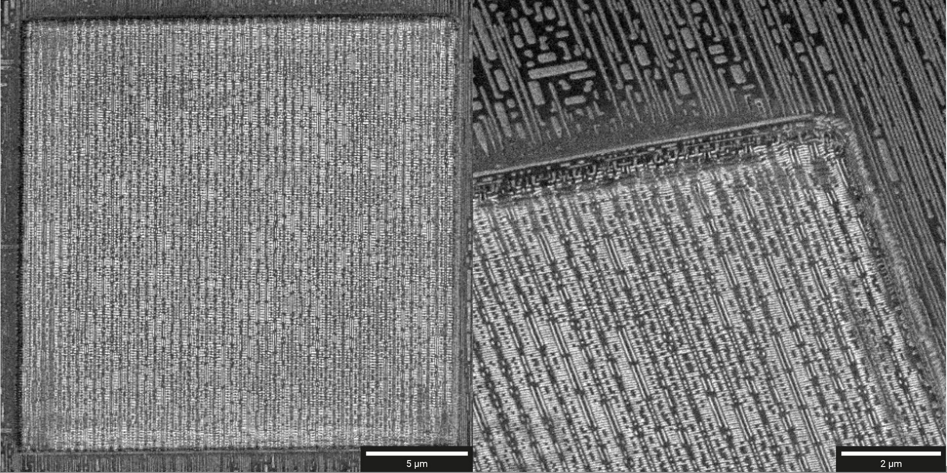
- (Left) Overview of delayered area (20 × 20 μm²) down to via contact layer. (Right) Detail showing smooth polished walls.