Failure analysis of semiconductor devices typically involves TEM inspection which requires routine TEM sample preparation in FIB-SEM machines. Such TEM samples should be site-specific with thicknesses comparable to the technology node of the inspected device. This imposes high requirements to a FIB-SEM machine in terms of performance and capabilities of the both columns: ion column for precise milling, and electron column for precise end-pointing. The new TESCAN S9000G FIB-SEM is the ideal platform to implement the most advanced techniques for TEM sample preparation, making it possible to fabricate thin lamellae with thicknesses of less than 10 nm.
Download the new TESCAN Application Example and find out more information.
-
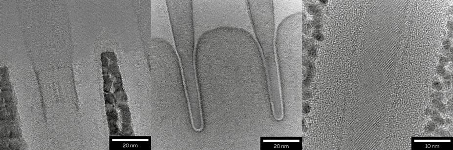
- TEM images of thin specimens prepared from a 10 nm node technology-based IC: (left) Gate-cut (center) Fin-cut (right) Cross TEM lamella showing thickness of < 10 nm.