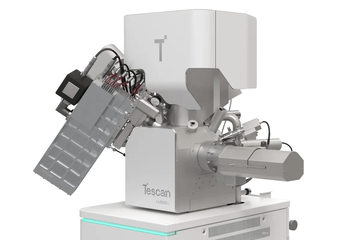
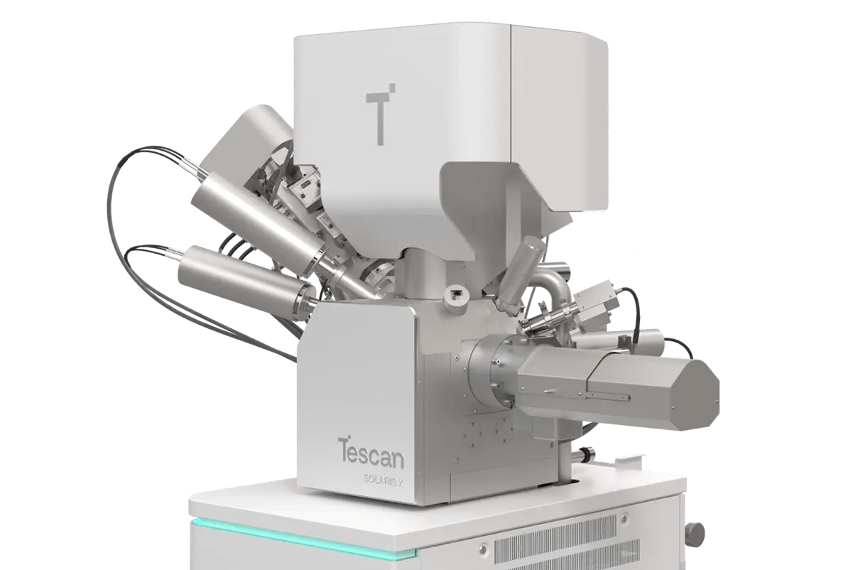
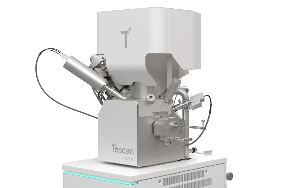
TESCAN
menu
en

Micro-Electro-Mechanical Systems

Micro-Electro-Mechanical Systems (MEMS) is a technology which can be defined most generally as miniaturised mechanical and electro-mechanical elements which are commonly made of Si substrate and fabricated by means of photolithography and chemical etching.

Semiconductors

Micro-Electro-Mechanical Systems

The critical physical dimensions of MEMS devices can vary from well below one micron, on the lower end, to several millimetres. Micromechanical switches in communication circuitry for phase shifting and signal switching and micro-mirrors for redirecting light or for correcting distortions due to air refractions or lens anomalies are typical examples of MEMS devices. MEMS are present in our daily life in many ways such as airbag and navigation sensors in vehicles, disk drive heads, inkjet printer heads, orientation detection in smartphones, or pacemakers and blood pressure sensors.

Overview of a MEMS sample (WideField mode)

  • SEM is an ideal technique by which we can inspect and localise failures and their root causes in MEMS.
  • High resolution and large depth of focus are capabilities that make TESCAN SEMs excellent instruments to observe samples with complex topography such as MEMS.
  • The ultra-high-resolution at low accelerating voltages enabled by MAIA3 can assist in the detection of small particles and other contaminants that may lead to device failure.
  • The high performance of the MIRA electron column allows for the examination of cracks, fractures or other signs of fatigue or wear in MEMS with moving parts or impact surfaces.
  • Many MEMS devices are securely packaged in order to protect their fragile elements.


Get in touch

Do you wish to discuss Micro-Electro-Mechanical Systems applications? Contact our Team directly!