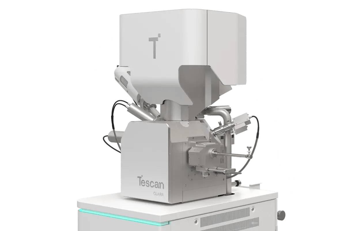
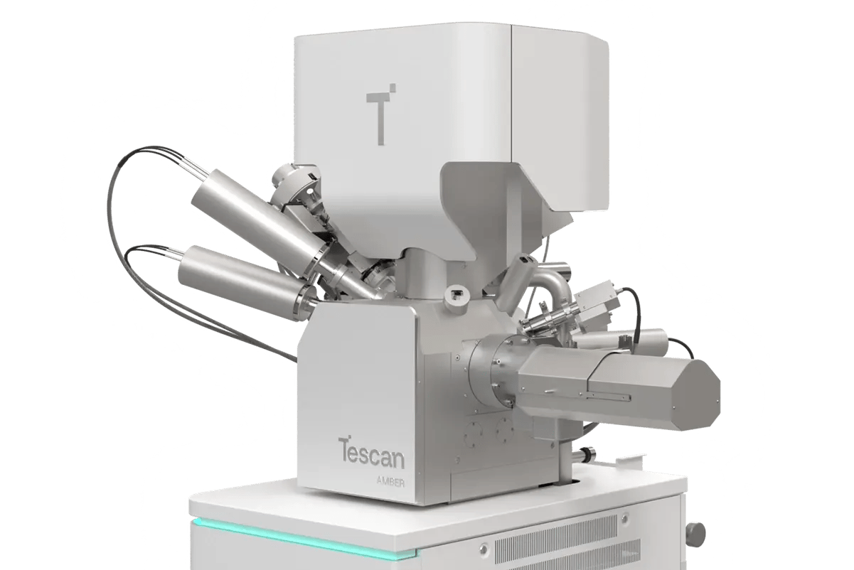
TESCAN
menu
en

Because everything needs to be just right

SAFINA, a.s. a company located right at the heart of Europe has developed from a small company with just a few employees into one of the leader manufacturers of metal powders. TESCAN is proud to support this company and their success through its product and application excellence.

Because everything needs to be just right

Fast developing, increasing needs
An increasing demand for metal powders used in additive manufacturing (AM) has led to a rapid growth of metallic powder producers which dedicate great efforts to developing new powder manufacturing methods and a wider range of products with diverse characteristics to satisfy specific needs and industrial applications. Powders have a high surface-to-volume ratio, a feature which makes metal powders useful as catalysts in many chemical or metallurgical reactions. Examples of these are silver (Ag) powders. Ag powders are classified according to their physical and chemical properties which can be tailored to meet customer needs. When manufacturing powders, the main parameters of interest are the average size of particles, particles size distribution, degree of purity, shape, density, tap density (after the powder being pressed), surface area, grain size, behaviour when exposed to heat, etc. Each of these properties has impact on the end-user application, and that is why it is important to have a strict control and a monitoring system in place.

A leap into the microworld
Powders consist of particles whose sizes are in the range of just a few microns up to a few hundreds of microns (a micron (µm) is the thousandth part of a millimetre). To have a better grasp of what this means, the diameter of a human hair ranges between 30 µm and 100 µm. An imaging technique compatible with the sizes of these microstructures is needed in order to explore features of interest and extract the maximum possible information of the samples. Optical microscopy is limited in the sense that it can only achieve object magnifications of up to a few hundreds or thousands times and, reduced depth of focus (essential feature for imaging samples with high topography); thus important structures of powders cannot be visualised with such microscopes.

To this end, scanning electron microscopy (SEM) is a powerful analytical technique well-suited for metal powder characterisation. SEM provides high magnification (that can be up to 1,000,000 times), high-resolution images with high topographic (with large depth of field) and material contrast that allow determining particle size and shape. These microscopes are fitted with a controlled source of electrons that are then focused to form a tiny probe with which the sample’s surface is scanned. During scanning the sample, electrons from the probe interact with atoms of the sample which originates the emission of different signals such as electrons, light and X-rays with different energy ranges. These signals are collected to form sample images. Furthermore, chemical composition of samples can also be analysed by means of collecting so-called characteristic X-rays. No doubt, SEM provides valuable analytical capabilities for metallic powder characterisation. In addition, dedicated software fully integrated into the microscope software platform can be used for obtaining particle size distribution and measuring particle size and surface areas.

Right at the heart of Europe
SAFINA, a.s. a company that processes and manufactures products made of precious and non-ferrous metals offers – among an extensive product line – a wide range of metal powders including Ag and Ag-coated metal powders which are especially aimed at additive manufacturing (AM). For their production, SAFINA uses the whole spectrum of powder manufacturing techniques such as gas atomising, hydrometallurgical processes and, a newly developed core-shell technology for coated metallic powders. Currently, a physical vapour deposition (PVD) technique for coating powders is under development. SAFINA also produces coated powders which are prepared by an electrodeless wet chemical coating process. Silver is a common coating for metallic powders. Ag-coated powders are commonly used in industry as a way to reduce production costs while keeping electrical and thermal conductivity properties at the level comparable to pure silver powders.

Because everything needs to be just right
SAFINA, a.s. offers competitive powder products under a flexible scheme which ensures minimum delivery times and tailored-made powders to meet specific needs, all of this at the highest quality standards. High quality is something SAFINA takes very seriously. All SAFINA’s products undergo strict control quality processes, and this is not the exception for metallic powders. To this end, SAFINA makes use of the most advanced analytical techniques thus guaranteeing word-class quality standards. In powder-based manufacturing processes, the determination of particle size, particle size distribution and morphology is essential since these powder characteristics have considerable effects on the properties of the final manufactured products including mechanical strength, porosity, and surface finish. The chemical composition and microstructure of powders have also their fair share in determining final quality in AM.

Installation of the TESCAN VEGA3 SB EasyProbe at the quality control facility for metallic powders in SAFINA

The laboratory for metallic powder control quality in SAFINA is equipped with a TESCAN VEGA3 SB EasyProbe. The TESCAN VEGA SB EasyProbe is a thermionic emission scanning electron microscope equipped with an energy dispersive X-ray spectrometer (EDS) which is fully integrated into the microscope software platform. The microscope in SAFINA is also fitted with a secondary electron (SE) and retractable backscattered electron (BSE) detector (in optical microscopy light rays are used to observe samples while in SEM electrons (SEs and BSEs) emitted from the sample as a result of the scanning are detected to form images). The SE detector provides high-resolution images useful for determining shape and size of powder particles while the BSE detector provides excellent material contrast. The EDS spectrometer makes it possible to analyse in detail chemical composition of the powder samples with high precision. This is possible because while scanning the sample with SEM not only electrons but other signals such X-rays are also emitted. X-rays carry valuable information on the chemical composition of the sample.

The SEM microscope in SAFINA is operated by Dr. Peter Pikna who is a Technologist/Development Specialist in SAFINA and the person in charge of control quality of metallic powders. Peter analyses powder samples where he verifies that the size of the powder particles are according to the specification whose size can be in the range of just a few microns up to tens of microns. “Customers often require a specific size of metal particles and we must make sure that the powder meets exactly the requested parameters” explains Peter.

Getting hands on powder samples
“The preparation of the sample for SEM analysis is pretty simple and straightforward,” says Peter while putting lab gloves on his hands to then sprinkle the powder to be analysed onto a C tape which in turn he has previously glued onto the sample holder. A simple and straightforward sample preparation for SEM analysis is indeed, one of the additional advantages of this imaging technique.

Preparing a powder sample for inspection and analysis in the scanning electron microscope TESCAN VEGA3

For Ag-coated powder microanalysis, Peter makes use of the TESCAN EasyEDX software, an easy-to-use software module that fully integrates the EDS detector into the TESCAN SEM VEGA3 control system. With this software, powder samples can be quickly and effortlessly analysed in a matter of a few seconds thus Peter can determine the quality of the Ag coating on the Cu powder; i.e. whether the coating is uniformly distributed on the surface of the Cu particles or not. For this, he selects different areas in the sample, scans and looks at the individual elemental distribution maps. Distribution maps as the name implies, shows the chemical composition of the sample and how each element is distributed. For this, the chemical elements are colour-coded by the software thus making element discrimination easy. EDS microanalysis is used to determine the chemistry of the powder particles, the advantage of this method compared to other chemical analytical techniques is that it is very fast and it allows point and line scans, and elemental analysis mapping. “This microscope (TESCAN VEGA) fully satisfies our analytical needs and, up to now we haven’t had any problem with it. We are very proud that we are one of the few companies in the Czech Republic that make use of SEM techniques for control quality. It is the ideal technique for sample analysis and control quality for our type of applications”, added Peter.

Performing diverse sample analyses: SE imaging for size and shape characterisation and EDS microanalysis for chemical characterisation and coating quality control

The TESCAN VEGA3 SB EasyProbe is a versatile microscope that can be used not only for powder analysis but also for other multiple applications in materials science. This microscope can also be configured to be compatible with low vacuum operations, a suitable feature which is useful when imaging and analysing any type of non-conductive samples.

Companies Profiles

SAFINA, a.s.
SAFINA is one of the leaders in the production of materials containing precious metals in Central and Eastern Europe. The main activities of the company include waste management and handling of materials, which contain precious metals. SAFINA is also a producer of a wide range of products made from precious metals and special alloys used in medical and other industries. Currently, Safina is expanding its market share in Europe as well as in North America, Asia, and Russia. SAFINA is a member of Plaurum Group incorporates production facilities in Russia (JSC EZOCM, OAM UZCHR, LLC UZCHP), Central Europe (SAFINA), United States (SAFINA Materials Inc.) as well as branches in Slovakia, Poland, Romania, and Kyrgyzstan.

TESCAN
TESCAN is a multi-national company and a leading global developer, manufacturer and supplier of scanning electron microscopes (SEMs), focused ion beam (FIB) systems and dual beam systems (FIB-SEM) as well as advanced quantitative phase imaging (QPI) microscopy. TESCAN specialises in unique solutions for SEM and FIB-SEM applications. Dedicated detectors as well as high performance software and imaging tools in the field of charged particle optics are also part of TESCAN portfolio. With headquarters in Brno, Czech Republic, TESCAN’s more than 25-year experience in the field of charged particle optics and over 2800 SEMs installed in more than 80 countries bear testament to TESCAN’s world-class quality, proven technology and continued service excellence.

26.07.2017