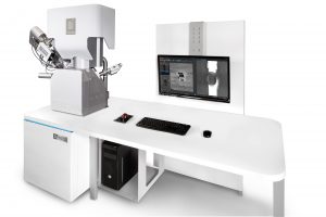
We are now pleased to invite you to attend a webinar dedicated to present the key features and typical application examples of this powerful new microscope. The TESCAN S9000X is fitted with the new iFIB+™ Xe+ plasma FIB capable of generating high ion beam currents and an unmatched field of view that redefines conventional large-area FIB cross-sectioning while slashing sample preparation time.
TESCAN S9000X is the platform for the most challenging physical failure analysis applications in semiconductors and material characterisation that require ultimate precision and extremely high-throughput. The TESCAN S9000X guarantees ultimate resolution and surface sensitivity essential to resolve nanosized structures, provides best conditions for large-volume 3D sample characterisations, and at the same time, it delivers unmatched FIB capabilities that enable precise, damage-free, and extremely large-area cross-sectioning in packaging technologies and optoelectronic devices.
The webinar will take place on Thursday, August 30, 2018, from 9 am to 10 am CEST and from 5 pm to 6:00 pm CEST. Register to join our webinar on TESCAN S9000X plasma FIB-SEM.
The registration is closed.