Copper pillar bumping is intended as a replacement to traditional solder bumping. In the solder bump process, a bump is formed on the chip and on the package substrate and they are connected by reflow. During the reflow the solder bumps collapse and do not retain their height in two directions. Moreover, the solder bumps occupy a larger space than the pitch of a pad on the chip. Copper pillar technology promotes a fine pitch, flip chip process, which is vital for today’s and future’s portable devices.
Cross-sectioning plays a central role in failure analysis in the semiconductor industry of copper pillar and other packaging technologies in microelectronics. The TESCAN XEIA3 Xe plasma FIB-SEM microscope and equipped with the Triglav™ UHR SEM column is an ideal platform to prepare and inspect copper pillar cross-sections in search for nonwetting, delamination, and other typical characterisations in failure analysis of these structures.
Download the new TESCAN Application Example and find out more on this.
-
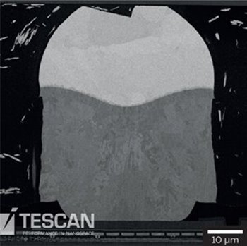
- Overview of the Cu pillar imaged at 5 keV with the Low-Energy BSE (LEBSE) detector showing strong material contrast between SnAg, Ni, Cu and the Si substrate
-
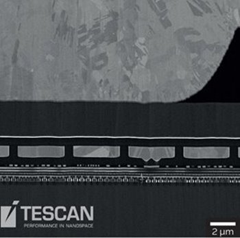
- Right corner of the copper pillar. Imaged acquired at 5 keV with the LEBSE detector shows channelling grain contrast on Cu forming the base of the pillar and top metal Al layer.