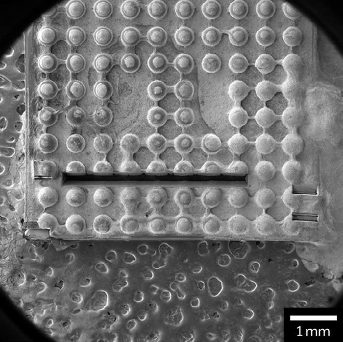
TESCAN’s Jozef Vincenc Oboňa, Product Marketing Director for Semiconductors, says that hybrid laser/FIB tools will become an integral part of analytical workflows in the semiconductor industry. Hybrid systems use the laser to remove the bulk of the material and FIB for final cross-sectioning and are integrated through correlative image alignment procedures and CAD overlay navigation. For large, high quality cross sections, calculated time savings compared to preparation with Plasma FIB alone range from 70% to 95%.
Read Jozef’s article that was published in Semiconductor Packaging News in January 2022 here.