Organic Light Emitting Diodes (OLEDs) is a flat light emitting technology, consisting of a series of organic thin films placed between two conductors. OLED displays are nowadays produced in mass for mobile phones, tablets, TVs, and wearables. Physical failure analysis of OLED/AMOLED displays can be quite tricky due to the presence of a large variety of materials such as polyimide, ITO, glass, organic layers, Al electrodes and other metals whose physical properties differ significantly from each other. These materials are placed in the form of very thin films whose thicknesses can range even in the nanometer scale. The TESCAN S9000X is a Xe plasma focused ion beam scanning electron microscope that has it all for preparing large-area cross-sections in displays that can be as large as 1 mm-wide, and at the same time, provides high resolution and excellent contrast at low beam energies required to image and resolve such delicate and small structures in displays.
Download the new TESCAN Application Example below and find out more information.
-
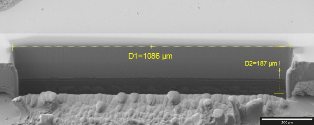
- 1086 mm-wide cross-section through part of an OLED display, SE detector at 2 kV
-
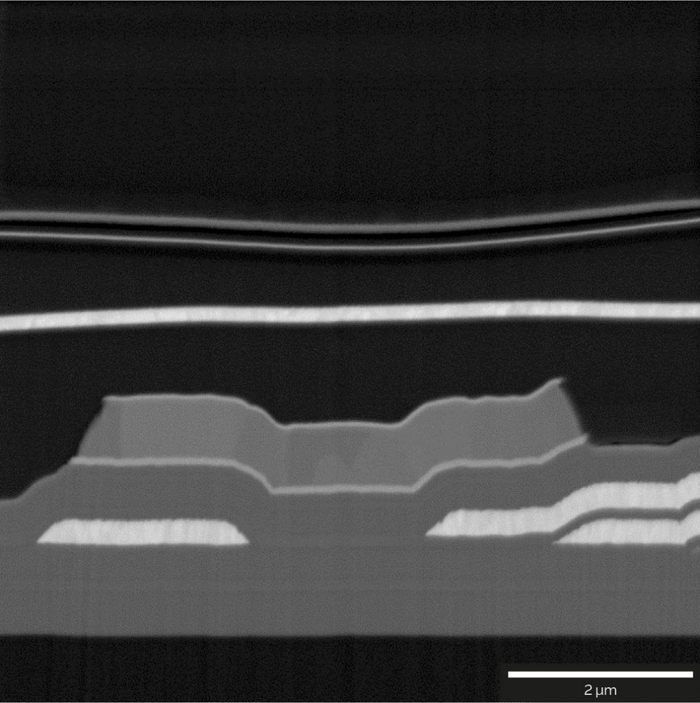
- Detailed image of the Al contacts and SiO2/SiNx layer structure. Mid-Angle BSE detector at 2 kV