Nanowires are of great interest because of their promising electronic and optical properties, which make it possible to manipulate light. Of special interest are nanowires based on group-III nitrides such as GaN since they are semiconductor materials with a wide band gap. The TESCAN S8000 offers excellent imaging capabilities and excellent performance at low electron beam energies essential to resolve morphological features of nano-sized structures. In particular, the TESCAN S8000 can help reveal surface morphologies of grown structures and provide plan views of GaN nanowires and quantum wells grown on the facets of nanowires.
Do you want to know more? Please see below on AE.
-
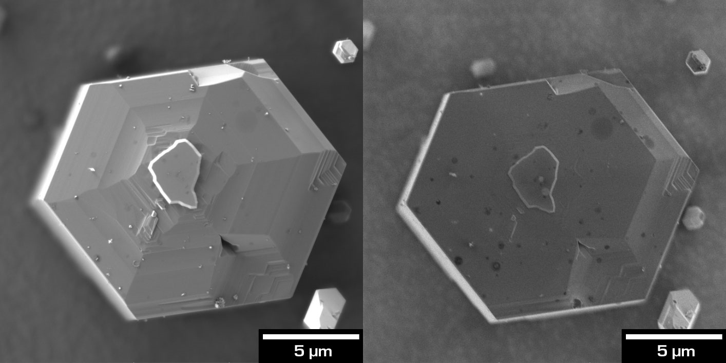
- Plan-views of GaN nanowires with InGaN quantum wells. Different BSE contrast acquired at beam energy of 2 keV with (left) the E-T detector for topographic contrast and (right) the Multidetector with grid ON set at -1.9 kV which filters out most of the bulk BSE revealing surface features that are not visible to other detectors.