TESCAN
menu
en

Plasma FIB and failure analysis in semiconductors

Visualization of doped active regions in semiconductor devices

Plasma FIB and failure analysis in semiconductors

Visualization of doped active regions in semiconductor devices

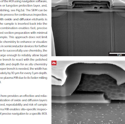
The described approach provides an effective and reliable solution for the visualization of oxide and diffusion layers in terms of accuracy, speed, repeatability and risk of sample damage. Plasma FIB enables site-specific inspection with the possibility of precise navigation to a specific region of interest.


09.03.2017
  • Visualization of doped active regions in semiconductor devices

    pdf 1 MB Download