Scanning Electron Microscopes (SEM)
Tescan’s SEM platforms provide high - resolution imaging and surface analysis with exceptional contrast, detail, and ease of use - ideal for materials research, quality control, and analytical applications.
Tescan’s portfolio spans SEM, FIB-SEM, 4D-STEM, and microCT systems - designed to serve advanced research, development, and quality control. From nanofabrication and TEM sample prep to non - destructive 3D imaging, our instruments combine precision, flexibility, and application depth across every major scientific and industrial domain.
Whether you're solving challenges in failure analysis, technology pathfinding, or process optimization, Tescan systems adapt to your goals - today and in the future.
Tescan’s SEM platforms provide high - resolution imaging and surface analysis with exceptional contrast, detail, and ease of use - ideal for materials research, quality control, and analytical applications.
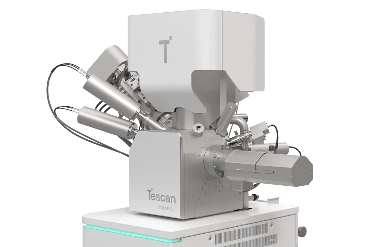
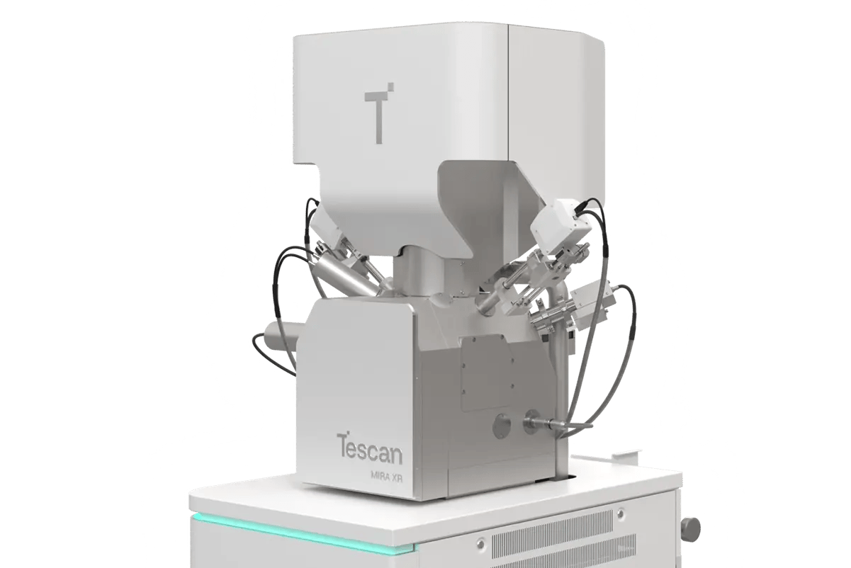
Tescan FIB-SEM systems combine fast, precise milling with high - resolution imaging and advanced automation. Choose from Ga+ or Xe plasma FIB sources to match your needs in sample prep, prototyping, or failure analysis.

Tescan’s X - ray micro-CT systems deliver fast, high - resolution 3D and 4D imaging for non - destructive internal analysis. Dynamic in - situ capabilities and modular designs make them ideal for advanced research across materials, life sciences, and energy storage.
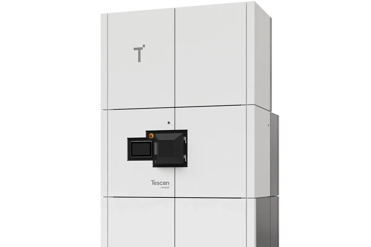
Tescan's TENSOR is the first fully integrated and synchronized analytical STEM platform built for intuitive multimodal nanocharacterization of a wide variety of samples, combining structural, morphological, and chemical insights. It is optimized for high-resolution crystallographic and structural analysis enabling full microscope automation, on-the-fly data processing for interactive analysis of samples, and scripting of new workflows that all together make it ideal for both routine and advanced research.

FemtoChisel is the next - generation femtosecond laser solution built specifically for semiconductor sample preparation and failure analysis. For too long, the industry has had to compromise between throughput, precision, and Surface Quality. Now all are delivered on one integrated platform.

Tescan EXLO is designed for laboratories where TEM throughput, reproducibility, and cost efficiency matter. By moving specimen lift - out outside the FIB-SEM, EXLO keeps valuable beam time focused on milling, while parallelizing lamella transfer and grid mounting. The result: higher output, lower cost per specimen, and a more efficient workflow.
.webp?width=415&height=400&name=NANOSPACE%20w600%20(1).webp)
Tescan’s advanced systems support operation under demanding conditions-from controlled ion implantation to analytical tasks performed in ultra-high vacuum environments-while offering the freedom to customize system configuration and workflows to your specific research needs.

Looking for the right solution for your research or application? Our specialists are here to help. Use the form below to book a consultation and discuss your needs, questions, and challenges. Together, we’ll explore the best options and see how Tescan can support you in achieving your goals. We’re always ready to listen and find the most effective solution for you.