One of the reasons is that the automatic wire bonding procedures are highly reliable and give high yields. The highest quality in terms of uniformity of wire properties is required; homogeneous chemical composition and stable mechanical properties in wires are desirable. Such wire properties can be altered or affected by the applied heat during the soldering process of the wires to the wire pads. The wiring area affected by the heat becomes mechanically weaker which can alter wire loop formation and its stability.
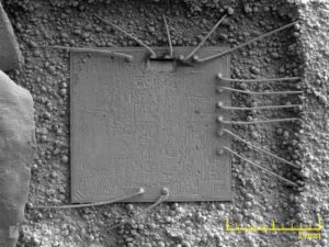
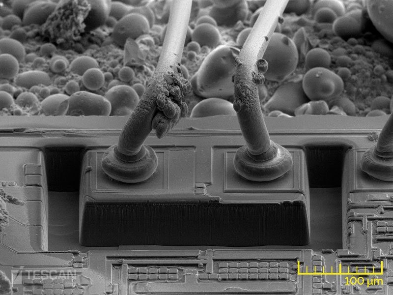
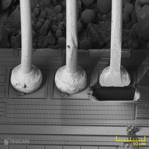
Overview of wire bonding on a semiconductor chip after chemical decapsulation
- SEM techniques allow for performing different tests on bonding wires. TESCAN’s patented aperture-free Wide Field Optics™ allows for the imaging of extra-large objects such as a whole chip package with exposed wire bonds at low magnification.
- The high-performance electron column of MIRA enables high electron currents which are favourable for implementing analytical techniques such as EDX and WDX. These are essential in order to conduct metallurgical studies of the bond wires in order to examine the formed intermetallic layers present at the bond wire interfaces, or, the influence of grain size distribution on the bonding process.
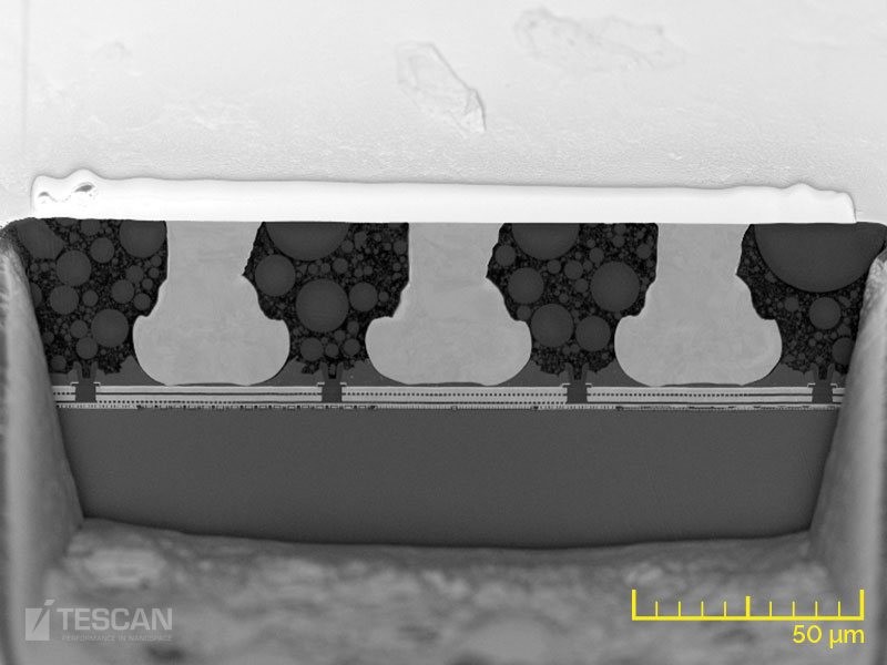
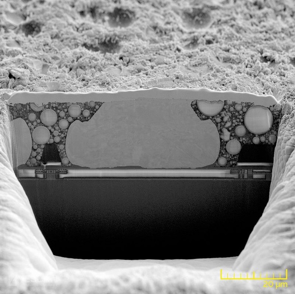
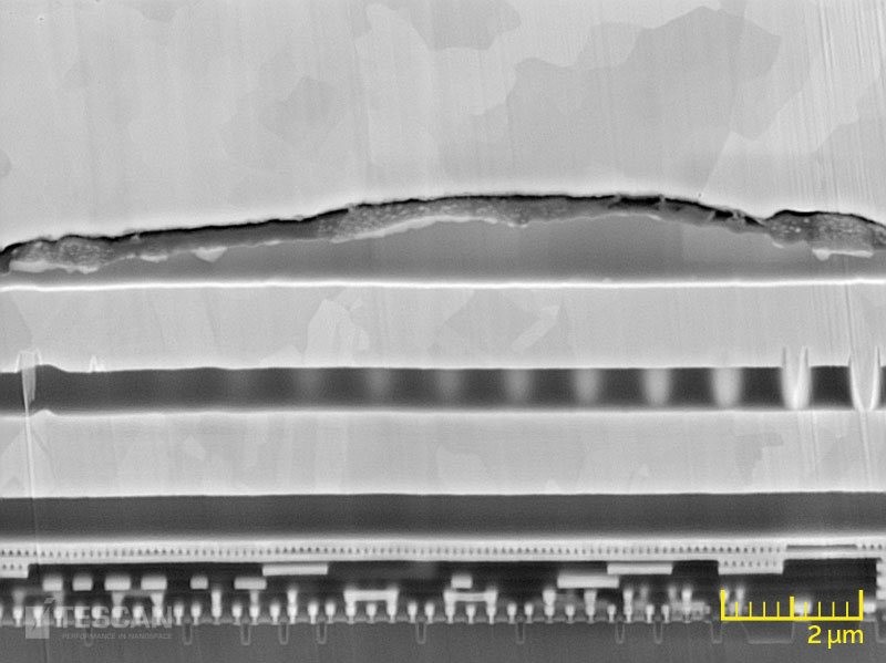
- TESCAN FIB-SEM systems extend the analytical possibilities by enabling nano and micro-engineering, a capability that allows for the cross-sectioning of bond wires to examine bondability and metallisation.
- SEM physical evaluation and FIB cross-sectioning can be also used to study the effect of high temperatures on bond wires such as metallurgical changes, voids and decrease in bond strength.
- Additionally, the TESCAN tensile stage and a nano-indentor can be used to perform in-situ stress tests in wires and wire bond quality.
- Different cross-sections prepared by Xe plasma FIB: A trench prepared for 3D tomography
- Crosssection of a ball bond and bond pad
- Wire bonds embedded in resin
- Cross-section ball bonds embedded in resin
- Magnified image of Cu bond showing a crack at the interface causing failure


