Discover Tescan’s

Advanced SEM
Scanning Electron Microscopes

Tescan SEM (Scanning Electron Microscope) systems deliver high-resolution surface imaging and analytical versatility for research, industrial quality control, and failure analysis across a broad range of applications.

Combining advanced electron optics with intuitive workflows and flexible analytical integration, Tescan SEM platforms enable users to investigate materials and structures from the microscale down to the nanoscale with speed, precision, and confidence.

Built on decades of expertise in electron microscopy and charged particle optics, the Tescan SEM portfolio supports applications spanning materials science, semiconductors, battery research, metallurgy, geology, life sciences, and additive manufacturing. From routine imaging and particle analysis to demanding low-voltage characterization and in situ experimentation, Tescan SEM solutions are designed to adapt to evolving scientific and industrial challenges.

The portfolio includes thermionic SEM systems for accessible and reliable routine analysis, as well as advanced field emission SEM (FE-SEM) platforms optimized for ultra-high-resolution imaging, surface sensitivity, and analytical performance. Field-free imaging technologies, advanced detection systems, and low-energy beam capabilities allow users to examine beam-sensitive, non-conductive, and complex materials while preserving sample integrity and maximizing image quality.

Tescan SEM systems support a wide ecosystem of analytical and correlative workflows, including EDS, EBSD, WDS, Raman, cathodoluminescence, tomography, and automated image analysis. Modular architectures and open platform design enable laboratories to configure systems around their specific applications while maintaining flexibility for future expansion.


Not sure which SEM configuration best fits your application, workflow, or throughput requirements? Request a personalized consultation with a Tescan specialist to discuss your samples, analytical goals, and laboratory needs, and identify the solution best suited to your research or production environment. 

VEGA LM Mat Science
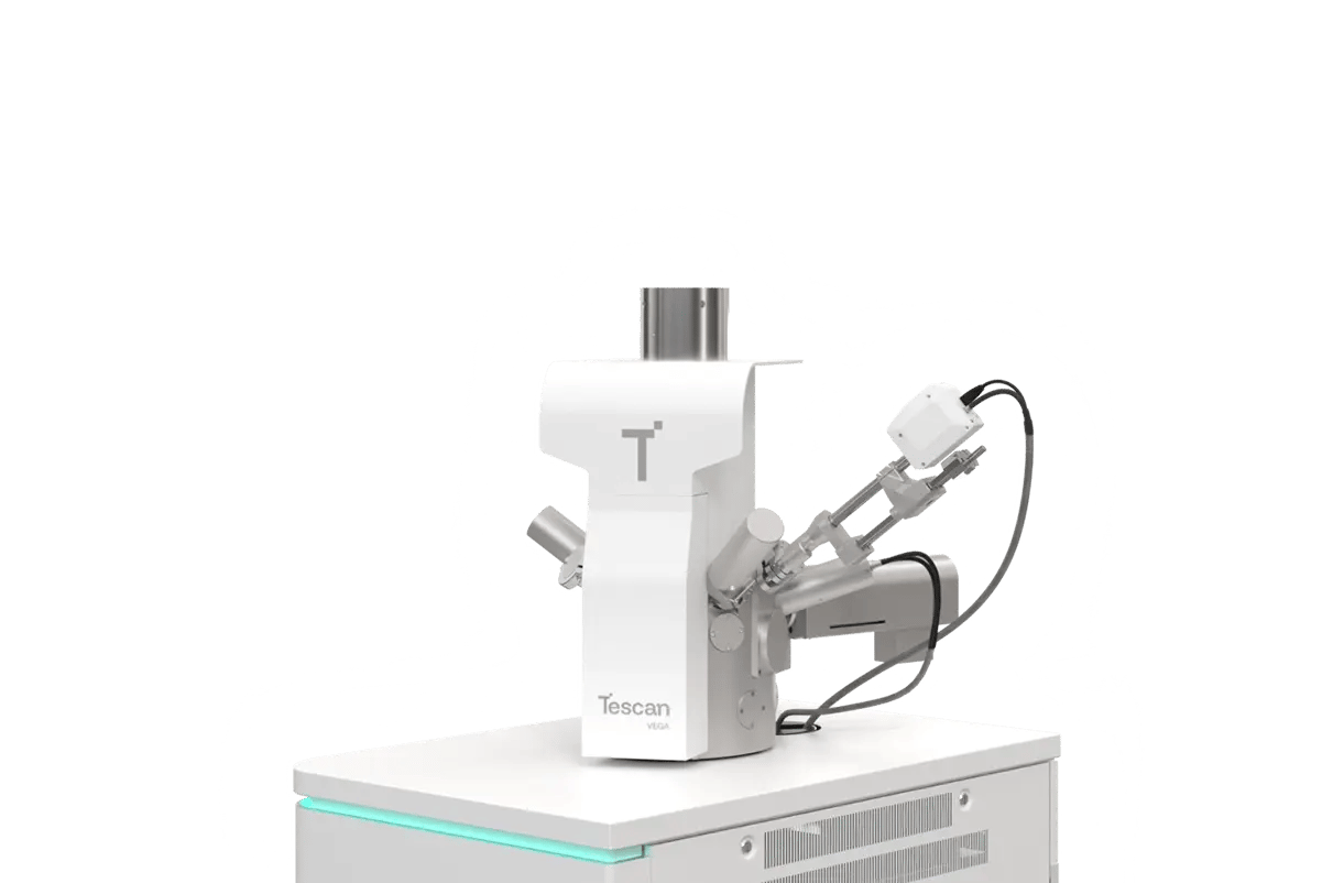
Tescan VEGA™

Tungsten SEM for routine imaging and analysis

Tescan VEGA provides high-resolution imaging and integrated EDS in a compact, aperture-less SEM system optimized for ease of use. With Wide Field Optics® and minimal training requirements, it enables fast navigation and operation for everyday materials analysis.

Key benefits

  • Fast start-to-data: 2× navigation speed and zero alignment steps — ideal for new or infrequent users.
  • Lower ownership costs: Long-life tungsten source and no aperture handling.
  • Simplified workflows: Integrated SEM–EDS analysis in a single, intuitive interface. 
VEGA Compact (3)
Tescan VEGA compact™

Compact analytical SEM for routine materials analysis

Tescan VEGA Compact delivers high-resolution imaging and integrated EDS in a simplified, space-efficient system. Researchers benefit from Tescan Essence™ software and a large chamber designed for industrial-scale samples, both supporting reliable, everyday materials analysis.

Key benefits

  • Large-sample capacity: A spacious chamber and stable high-vacuum conditions support efficient analysis of large or multiple samples with dependable EDS results.
  • Fast beam optimization: In-Flight Beam Tracing™ helps you set optimal beam conditions quickly.
  • Integrated EDS correlation: Essence™ EDS overlay tools let you view morphology and composition together in one intuitive interface.
MIRA LM Mat Science
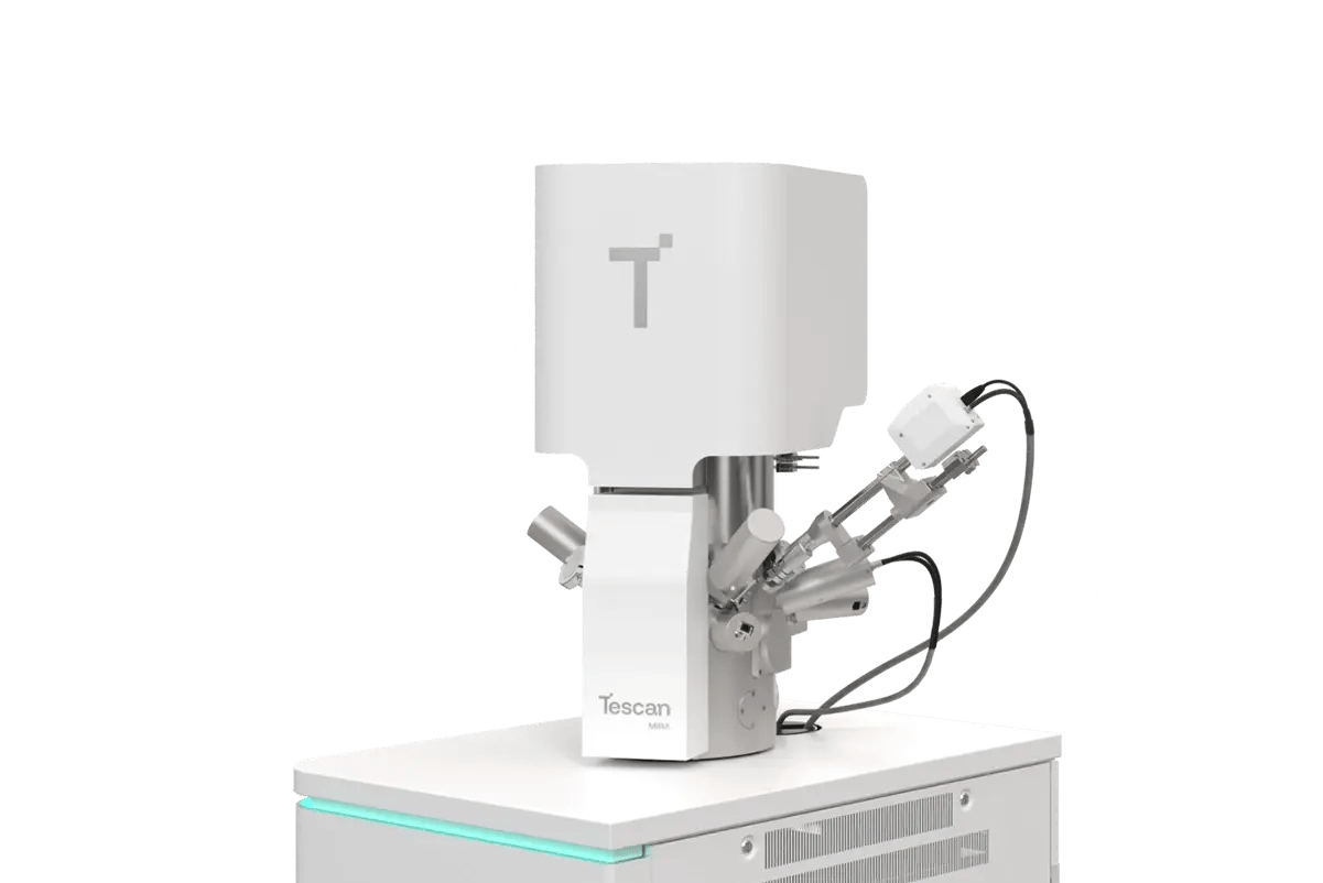
Tescan MIRA™

Modular FEG-SEM for analytical research and failure analysis

Tescan MIRA gives you high-current, high-resolution imaging with Schottky FEG optics and support for EDS, EBSD, CL, STEM, and nanoprocessing. Its modular design and upgrade options let you expand capabilities as your analytical needs grow in research and QA/QC.

Key benefits

  • Faster beam setup: In-Flight Beam Tracing™ and Wide Field Optics® support quick beam optimization and smooth navigation
  • High-throughput analysis: Stable performance for advanced EDS/EBSD mapping and compositional workflows
  • Expandable platform: Modular hardware and correlative method support help labs adapt to evolving analytical requirements.
MIRA XR GM MONO Metal
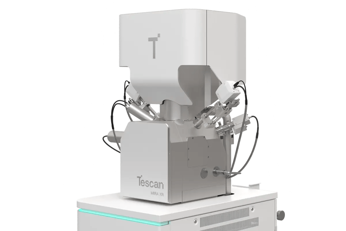
Tescan MIRA XR™

UHR FEG-SEM for shared labs and quality control environments

MIRA XR gives you BrightBeam™ UHR optics, Wide Field Optics®, and Dual Essence™ EDS for high-resolution imaging and live compositional analysis. Designed for diverse users, it handles charging, non-conductive, and outgassing samples with confidence.

Key benefits

  • Reduced rework and training time: Macro-to-nano navigation and automated beam optimization help you reach the right settings quickly.
  • Nanometer-scale detail at low keV: Advanced SE/BSE detection and automated column alignments support your high-resolution imaging and analysis.
  • Higher throughput on challenging samples: MultiVac™ and Auto LowVac Aperture give you more control and stability when working with difficult materials.
CLARA GM Mat. Science
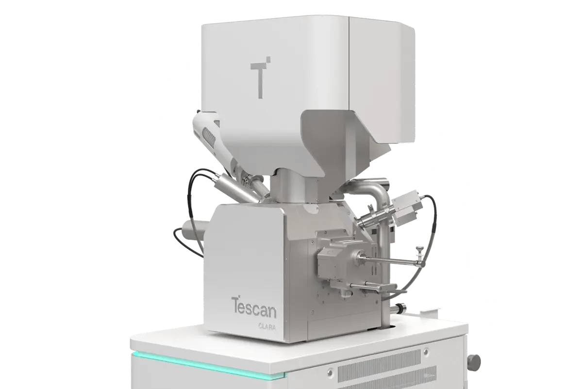
Tescan CLARA™

Field-free UHR SEM for high-contrast imaging of sensitive materials

Tescan CLARA gives you sub-nanometer resolution with BrightBeam™ optics and flexible detection options. Designed for delicate and non-conductive samples, it supports multimodal workflows and in-situ experiments with strong contrast at low keV.

Key benefits

  • Artifact-free imaging: Field-free optics and low-keV detection help you image magnetic, charging, and beam-sensitive samples confidently.
  • Selective insights in a single scan: Energy-filtered, in-column multi-detectors give you combined topography and composition information in one pass.
  • Support for advanced workflows: Modular hardware and open scripting options let you adapt CLARA to correlative and dynamic applications as your research evolves.
MAGNA GM Mat. Science
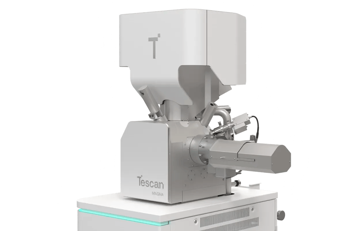
Tescan MAGNA™

Immersion UHR SEM for contrast-critical nanoscale imaging and STEM-in-SEM analysis 

Tescan MAGNA gives you TriLens™ immersion optics and energy-selective detectors that produce clear, unmixed contrast at high resolution. You can maintain image quality at long working distances and on tilted surfaces, enabling detailed analysis of cross-sections, nanomaterials, and complex failure features.

Key benefits

  • Clear SE/BSE contrast: TriSE™ and TriBE™ detectors provide well-defined signals so you can distinguish surface and compositional information with confidence.
  • High resolution at long working distances: Stable sub-nanometer performance supports your work on complex sample geometries and challenging orientations.
  • STEM-in-SEM capability: Integrated STEM-in-SEM lets you perform advanced nanoscale characterization without switching platforms.
TIMA GM
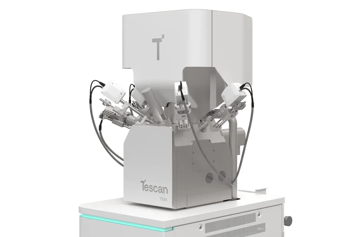
Tescan TIMA™

Automated mineralogy SEM for quantitative particle-by-particle analysis

Tescan TIMA gives you high-throughput SEM-EDS with automated mineral identification and textural analysis to provide reproducible, quantitative mineralogical data at scale. Its integrated correlative imaging and fully automated workflows support exploration, process optimization, and academic research while removing manual interpretation and user bias.

Key benefits

  • Robust mineral data: Four EDS detectors and spectral summing deliver rapid phase, texture, and liberation measurements, even for accessory and rare minerals.
  • Lower workload: Unattended acquisition, automated classification, and batch export reduce the time you need to spend on manual tasks.
  • Stronger process insights: Correlative imaging links composition with particle structure and spatial relationships to support exploration and process optimization.

GET IN Touch

BOOK A DEMO

Built around your needs

map

Where can you find us:

Tescan
Libušina třída 21
623 00 Brno
Czech Republic

130405923 us US 37.09024 -95.712891 25.3575 29.349345 20.67957527 42.082797 39.91384763 -33.693421 13.93320106 3.039986586 31.997988 38.050985 47.579533 48.1485965 58.375799 54.663142 19.195447 56.975106 47.916997 50.493053 45.868592 10.79556993 44.35660598 43.2371604 55.536415 14.557577179752773 32.100937 -6.116829 -6.212299277967318 33.600194 -12.08688 23.7104 -33.471062 31.998740087 -23.69149395 43.462349 51.529848 49.1893523 49.197486 25.072375 31.075811 1.299027 40.676979 52.30150662 51.013813 35.684121 37.566531 52.246622 40.581349 39.911632 -26.1811371 41.818215 33.429928

No distributors found.