The possibility of consistent and efficient inspection throughout the entire manufacturing process of semiconductor devices is one of the key attributes for high yields and profitability. Feedback on control of each manufacturing step is absolutely necessary, especially during the mass production of wafers (tens of millions of devices per week). Checking layer thicknesses, step coverage, geometry of critical details, depth of trenches, etc. is carried out in order to find defects, their origin and implement appropriate corrective measures. The approach described in this application example provides an effective and reliable solution for the visualization of oxide and diffusion layers in terms of accuracy, speed, repeatability and risk of sample damage. For this, the focused ion beam scanning electron microscope TESCAN FERA3 equipped with a Xe plasma FIB column and capable of 6”, 8” and 12” wafer handling is used enabling site-specific inspection with the possibility of precise navigation to a specific region of interest.
Do you want to find out more? Please download the Application Example from the link below.
-
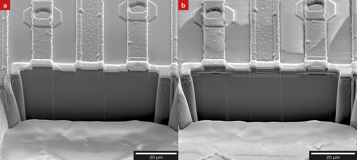
- (a) Cross- section before chemical treatment. (b) Crosssection after the etching procedure for the visualization of oxide and diffusion layers.