Advanced packaging technologies have been developed as a solution to pursue higher functionality, higher density and lower power consumption. Failure analysis of integrated circuit packaging usually requires preparing large area cross-sections. The new TESCAN S8000G FIB-SEM is equipped with the novel Orage™ Ga FIB column capable of a maximum ion beam current of 100 nA which makes it possible to prepare large-area cross-sectioning of solder balls in an automatic and precise way. This increases throughput in the workflow of failure analysis in packaging technologies.
Do you want to know more? Please see below on AE.
-
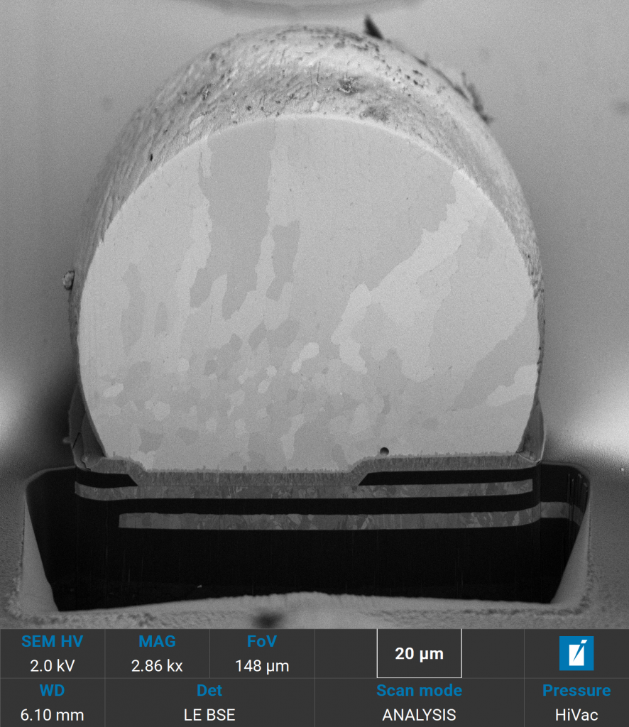
- SEM image of solder ball cross-section taken at 2 keV using BSE detector showing excellent material contrast.