Explore the Free Spring Seminar Series of TESCAN 2021
Join our Spring Seminar Series and extend your knowledge of the most innovative technologies in electron microscopy and micro-CT.
This free 12-seminar series will take place weekly, starting 3 March through 19 May 2021. The Series will feature leading technology & applications experts who will cover important topics in the geoscience, materials science, life science and semiconductor industry.
Check the individual topics below and register for free today!
Invitation to celebrate Paul Gottlieb’s career and contributions in Automated Mineralogy
Invitation to celebrate Paul Gottlieb’s career and contributions in Automated Mineralogy.
Presented by Dirk van der Wal, Product Marketing Director Materials and Geosciences for TESCAN
On January 1 of this year, Paul Gottlieb retired following 40 years of dedication to the development of Automated Mineralogy technology, systems, and applications, in collaboration with many of you, at institutions and companies across the globe. Please join us for a special 30-minute online event on March 3, in which we will celebrate Paul’s many contributions to Automated Mineralogy technology, hear stories from the early days in this field, and give you a chance to wish Paul and his wife Kay all the best in the next chapter of their lives. We look forward to having you with us as we give Paul the recognition that is so well deserved.
AUTOMATED MINERALOGY is an advanced, highly automated scanning electron microscopy/energy-dispersive x-ray spectroscopy (SEM/EDS) microanalysis application, and is possibly the earliest form of correlative microscopy. AM yields information about the textural relationships between minerals of interest, such as mineral association or liberation.
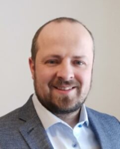
About Dirk van der Wal
Product Marketing Director Materials and Geosciences for TESCAN
www.linkedin.com/in/dirkvanderwal
Presenter: Dirk van der Wal
Date: Watch now on demand
Efficient Analytical Workflows with TESCAN's VEGA and MIRA SEMs
Feature size and its potential to deviate from expectation, materials composition, and the relationship between small scale and large scale — these are common questions that can be resolved by SEM microanalysis.
Samples may vary in type, size, and shape, as well as in their individual preparation methods, therefore, an SEM workflow is the best choice for obtaining characterization data. The most common SEM workflow consists of three steps: navigation, sample contrast exploration (SE/BSE), and elemental inspection (EDS). The degree to which this workflow can be effortlessly and efficiently applied to the wide range of samples coming to the laboratory—while also maintaining the highest possible resolution and image quality—is one of the many key factors which define the productivity and success of materials research and development projects.
At their market introduction, TESCAN´s VEGA and MIRA SEMs were designed to allow users performing this common workflow to do so intuitively and efficiently. In this webinar, we will show how new features on TESCAN’s 4th Generation VEGA and the FEG-SEM MIRA make a conventional analytical workflow more intuitive to perform as well as more efficient, so all users, even those new to SEM, can obtain comprehensive data.
About Petr Klimek
Petr Klímek is a Product Manager for TESCAN SEMs at the TESCAN ORSAY HOLDING in Brno, Czech Republic. He has 5 years of experience with SEMs and their application to routine microanalytical tasks. He obtained his Ph.D. in Materials Sciences at Mendel University in Brno and extended his materials research background through his internships at Fraunhofer WKI and Oregon State University (Fulbright Scholar).
Presenter: Petr Klimek
Date: Watch now on demand
Micro-CT and Additive Manufacturing: Moving from 3D to 4D
The evolution of additive manufacturing (AM) over the last decade has been impressive and looks to be revolutionary as a disruptive technique in the overall manufacturing arena. However, there are still a number of obstacles to overcome concerning the quality of the final part. Micro Computed tomography (micro-CT) is a non-destructive technique used to create highly detailed 3D volumes of intact samples and is widely used throughout an AM part’s lifecycle, including process development, process monitoring, and final part quality. TESCAN micro-CT products meet this challenge head-on; providing maximum flexibility and versatility, as well as opening up the possibility to perform 4D studies on samples.
In this seminar we will provide the basics of micro-CT, examples of imaging 3D printed samples, and discuss the future of micro-CT, and dynamic CT – where samples are continuously scanned at high rates while undergoing change, either naturally or induced. If you’d like to learn more about this exciting topic, please join us to see the possibilities that micro-CT brings to the additive manufacturing space!
About Jan Dewanckele
Jan Dewanckele is a Senior Application Scientist for TESCAN XRE at the micro-CT Technology Center in Ghent, Belgium. He has been active in micro-CT technology for more than 10 years, covering a broad array of applications with a clear focus on dynamic CT. He obtained a Ph.D. in geosciences at Ghent University (Belgium).
Presenter: Jan Dewanckele
Date: Watch now on demand
Faster mm-scale Semiconductor Failure Analysis by Combining Plasma FIB Milling and Laser Ablation
Improvements in performance and decreases in power consumption have long been the basic requirements in the design of electronic devices. These properties have been achieved through miniaturization of device building blocks (transistors, memory cells, etc.), reduction of the signal path (advanced integration of multiple components in one package), and optimization of other components, including displays, RF, MEMS, or batteries.
Developing new technology products is very challenging. Fast failure analysis (FA) significantly helps in determining defect root-cause and providing feedback to maintain feasible time-to-market and device reliability. FA in packaging, advanced packaging, displays, RF, MEMS, and batteries usually involves searching for a defect buried a few hundred micrometers or even millimeters under the surface. Due to the sensitivity of the structures, site-specific analysis of the defect is usually done in cross section and large amounts of material must be sputtered to get to the region of interest. Industry-proven plasma FIB technology has served these purposes for nearly 10 years. Recently, however, significant increases to both the complexity of the devices and the depth of buried defects, together with pressure on time-to-result have challenged even plasma FIB capabilities. Adding the thousands-times faster laser ablation technique to the plasma FIB sample analysis workflow speeds the time to premium results while also opening new synergies among other instrumentation in the FA laboratory.
This webinar will provide you with an introduction to the TESCAN Large Volume Workflow. The flexibility of the workflow will be demonstrated using demanding samples of different sizes, including complex devices and non-conductive hard materials. We will show how to achieve fast, artifact-free sample preparation results that are compatible with UHR SEM imaging for revealing the finest details.
About Jozef Vincenc Obona
Jozef Vincenc Obona is a Product Marketing Director for the semiconductor market segment at TESCAN ORSAY HOLDING HQ in Brno, Czech Republic. He obtained a Ph.D. in cryo-electronics at the Slovak Academy of Sciences (Slovakia). He has been active in semiconductor failure analysis (Front-End of the Line, Back-End of the Line and packaging applications) and extensively communicating with semiconductor industry leaders for more than 6 years. He has gained over 13 years of experience in FIB-SEMs and 5 years in ultra-short laser pulse processing in applied research at Instituto de Nanociencia de Aragon (Zaragoza, Spain) as well as University of Groningen and University of Twente (Groningen, Enschede, The Netherlands). He is the author of 3 patents and 52 publications.
Presenter: Jozef Vincenc Obona
Date: Watch now on demand
Introducing the new TESCAN TIMA for Geosciences
In November 2020, TESCAN announced the release of the new generation of TESCAN TIMA, a dedicated solution for automated mineralogical analysis in Earth Science studies as well as for industrial mineral processing. TIMA contributes to a wide array of applications ranging from petrography, metallurgy, liberation analysis, and provenance studies, even outside of geoscience.
TIMA is a user-friendly solution for executing petrographic workflows such as mineral identification and quantification, as well as localization of petrogenetically significant phases or their pairs based on their textural relationships, morphology, or association. TIMA can be the first step in complex analytical workflows followed by EPMA or LA ICPMS studies. TIMA is can be configured with an integrated Raman spectrometer, allowing direct identification of polymorphic modifications without the need to transfer the samples to other instruments. In addition to these features, TIMA also can provide a quantitative composition of both the individual mineral grains in relation to their morphology, as well as bulk composition of the entire sample.
In this webinar, we will focus on applications in geosciences and show how TIMA’s features and workflows support accurate, automated mineralogical analysis.
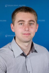
About Marek Dosbaba
Marek Dosbaba is a Product Manager for automated mineralogy at TESCAN ORSAY HOLDING in Brno, Czech Republic. Marek is with TESCAN since 2013. He has a background in mineralogy and the application of microanalytical methods on geological materials (electron microprobe, Raman spectroscopy, CL). He joined the application group first and switched to the product group at the beginning of 2019.
Presenter: Marek Dosbaba
Date: Watch now on demand
SEM Large-volume Analysis in Life Sciences assisted by Serial Block-Face Imaging
We are excited to present you our TESCAN brand-new solution in our Life Sciences product family, Serial Block-Face Imaging (SBFI).
Serial Block-Face Imaging (also known as Serial Block-Face SEM) is a traditional technique for high-resolution structural analysis of the sample using an integrated microtome to the SEM chamber. The method uses a diamond knife of the microtome to cut a slice from the sample surface (20-100 nm thin) which is immediately imaged by SEM. This process is repeated to create an image stack allowing a reconstruction of the sample volume.
In-chamber microtome device, compact size, simple and fast installation/de-installation, SEM / FIB-SEM GM chamber compatibility, effective LE-BSE imaging, and/or TESCAN volume analysis software – these are the key features that give us the opportunity to extend the capabilities of standard SEM to the volume scale of structural analysis. Key technical features of this exciting solution together with multiple application examples will be presented at the seminar.
About Ondrej Sulak
Ondřej Šulák received his Master’s degree in Analytical chemistry at Masaryk University in the Czech Republic. Then, he moved to France where he continued his Ph.D. studies and Postdoctoral research at Joseph Fourier University in Grenoble where he was focused on the structure-functional characterization of carbohydrate-binding proteins, mainly by X-ray crystallography, Electron Microscopy, SAXS, and other techniques. His industrial career started in the biotechnological company where he was responsible for the biochemistry department. In 2016, Ondrej joined TESCAN as Global Applications Director. Since January 2019 he works as Product Marketing Director for the Life Sciences segment.
Presenter: Ondrej Sulak
Date: Watch now on demand
Innovative FIB/SEM Lift-out Solutions for Advanced TEM Lamella Preparation Requirements
The success of transmission electron microscopy (TEM) analysis depends heavily on the quality of the sample preparation. And sample preparation requirements become more stringent when the atomic resolution is needed or when material features are smaller or more complex. Using FIB to prepare samples for TEM provides the best method for achieving the required thin lamella and ensuring uniform quality. Today’s novel materials, in particular, require more advanced TEM sample preparation methods to truly observe the samples with the desired detail.
For these novel materials, sample thickness is not the only parameter that must be considered. FIB-SEM instruments allow site-specific sample preparation by combining several techniques that help to locate the feature of interest on the sample or determine the orientation of a structure. In some cases, the samples will require that the lamella is prepared from a specific geometry, which necessitates the use of a lift-out technique.
In this webinar, you will learn how the unique position of nano manipulator in the FIB/SEM chamber supports innovative lift-out methods and unique geometries that are opening new possibilities for TEM lamella preparation as well as new opportunities for more advanced studies.
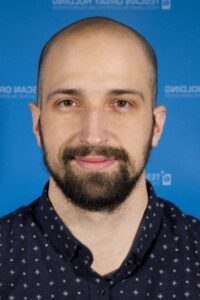
About Martin Slama
Martin Sláma is a Product Manager for FIB-SEM in Material Science and Life Science with over 5 years of experience in conventional and advanced TEM preparation methods using TESCAN’s plasma FIB and Ga+ FIB-SEM solutions for Materials Science. Prior to joining TESCAN, Martin worked in the field of new material development and characterization at Brno Technological University, CEITEC, and Aston University.
Presenter: Martin Slama
Date: Watch now on demand
Leveraging Advanced UHR-SEM Contrast Methods Using TESCAN CLARA's In-column Detectors
With the similarities in today’s UHR-SEM resolution performance specifications, the criteria for evaluating UHR-SEM capabilities, slowly but surely, are placing more emphasis on the ability to use multiple diverse contrast methods to reveal information that is not visible with resolution alone.
In general, when energy is transferred to the specimen by the primary beam, the sample generates a range of useful signals that are exploited to characterize the material. One of the principal signals generated by the sample, the backscattered electron (BSE) signal, originates at a range of angles and emitted energies from different depths below the sample’s surface. Thus, the angular and energy-selectivity characteristics of the BSE signal are considered secondary backscattered electron contrast methods. It is evident that having the ability to acquire the BSE signal selectively brings with it the potential to enhance the information that a backscattered electron image reveals.
In this webinar, we will show how TESCAN CLARA UHR-SEM is tackling the requirement for differentiated contrast methods by implementing a comprehensive choice of backscattered electron detectors, including chamber-mounted segmented solid-state or scintillator backscattered electron detectors, an on-axis in-column detector, and the proprietary in-column Multidetector™.
About Petr Klimek
Petr Klímek is a Product Manager for TESCAN SEMs at the TESCAN in Brno, Czech Republic. He has 5 years of experience with SEMs and their application to routine microanalytical tasks. He obtained his Ph.D. in Materials Sciences at Mendel University in Brno and extended his materials research background through his internships at Fraunhofer WKI and Oregon State University (Fulbright Scholar).
Presenter: Petr Klimek
Date: Watch now on demand
3D FIB/SEM Data Acquisition and Processing Solutions for Life Sciences
Current trends in electron microscopy include increased focus on the analysis of beam-sensitive biological materials such as tissue or cell cultures. Modern SEM column designs are able to acquire images at very low accelerating energies which are key for efficient visualization of these sensitive biological samples at scales approaching the nanometer range.
Combining scanning electron microscopy with the site-specific milling capability of the focused ion beam (FIB) opens a broader range of possibilities for studying biological samples. FIB-SEM systems are widely used not only for routine preparation of ultra-thin specimens for analysis in the transmission electron microscope (TEM) but also for precise cross-sectioning and 3D volume imaging in both ambient temperatures and cryogenic conditions. FIB milling is used extensively to reveal sub-surface information from bulk material or to create samples for other analytical modalities. Using FIB-SEM for 3D tomography is a powerful technique in structural biology for enabling visualization of diverse organelles and tiny structures which helps researchers answer questions about the principles of biological processes.
In the seminar, we will discuss the capabilities of FIB-SEM solutions for detailed structural analysis of biological samples, including recent trends for using plasma-based FIB-SEM solutions to revealing the highest details in large volume sample analyses.
About Martin Slama
Martin Sláma is a Product Manager for FIB/SEM in Material Science and Life Science with over 5 years of experience in conventional and advanced TEM preparation methods using TESCAN’s plasma FIB and Ga+ FIB-SEM solutions for Materials Science. Prior to joining TESCAN, Martin worked in the field of new material development and characterization at Brno Technological University, CEITEC, and Aston University.
Presenter: Martin Slama
Date: Watch now on demand
Introducing the new TESCAN TIMA for Mineral Processing
In November 2020, TESCAN announced the release of the new generation of TESCAN TIMA, a dedicated solution for automated mineralogical analysis in Earth Science studies as well as for industrial mineral processing. As a dedicated industrial mineral processing solution, TIMA is designed with the robustness required by the industry, while also minimizing the need for expert operators or even on-site presence thanks to its high level of automation and remote-control capability.
TIMA’s patented spectral summing algorithm not only increases throughput but also significantly enhances the detection of low abundance elements. TIMA automates mineral phase identification, measurement, and textural data interpretation and channels the results into predefined or highly customizable reports. Particle and grains filtering and categorization are available for advanced users, while data management workflows remain simple. Built-in quality control features produce reliable and robust data which can be processed offline to maximize the tool time for the automated runs.
In this webinar, we will focus on TIMA’s features and workflows listed and their role in high throughput industrial mineral processing.
About Marek Dosbaba
Marek Dosbaba is a Product Manager for automated mineralogy at TESCAN ORSAY HOLDING in Brno, Czech Republic. Marek is with TESCAN since 2013. He has a background in mineralogy and the application of microanalytical methods on geological materials (electron microprobe, Raman spectroscopy, CL). He joined the application group first and switched to the product group at beginning of 2019.
Presenter: Marek Dosbaba
Date: Watch now on demand
Prepare Top-down, Inverted and Planar TEM lamella from Logic and Memory Devices
Presented by Lukas Hladik, Product Manager for FIB-SEM systems in the Semiconductor market segment
The global integrated circuit (IC) industry is facing not only continuous growth in demand for electronic devices but also improvements to device performance and energy consumption—all while decreasing device footprint. In order to achieve this, TEM lamella preparation has become an inevitable part of the failure analysis process.
The 3D structure of today’s devices requires the localization of defects in different projections. The shrinking device size dictates the need to use inverted TEM lamella geometry to achieve sub-10 nm lamella thickness. With defect size now at the nm-scale, there is an additional need for plan-view TEM lamella geometry for STEM observation. Thus, TEM lamella lift-out procedures might require multiple manipulation steps or even breaking the vacuum to reach inverted or plan-view lamella geometries. TESCAN SOLARIS addresses these challenges with a patented setup that enables lamella transfer from a bulk sample onto a TEM grid with a single, simple manipulation step, and no need to break the vacuum or unload the sample. Most importantly, this approach does not require any additional hardware to be installed.
This webinar will provide you with insight into how TESCAN SOLARIS and its ecosystem can be utilized for semi-automated, high-quality, low beam damage sample preparation in the semiconductor FA lab environment.
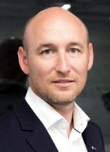
About Lukas Hladik
Lukas Hladik is a Product Manager for FIB-SEM, characterization, and delayering/probing solutions for FA semiconductor R&D labs. He joined TESCAN ORSAY HOLDING in 2012 as an application specialist for Plasma FIB-SEM platforms. All his work in TOH has been connected extensively with the worldwide semiconductor industry. Lukas has a Master’s degree in Physical Engineering and Nanotechnology from Brno University of Technology, Brno, Czech Republic.
Presenter: Lukas Hladik
Date: Watch now on demand
Cryo-TEM Lamella Preparation from Biological Samples
Low-temperature electron microscopy (cryo-EM) has become an established technique for capturing and observing beam-sensitive samples in their close-to-natural state.
Cryo-sectioning is a standard method used for thinning and slicing such samples. However, the integrity of the specimens can be degraded easily by common artifacts such as knife marks, compression, or crevasses. Focused ion beam (FIB), on the other hand, is used extensively to reveal sub-surface information from bulk material, create samples for other analytical modalities, or prepare ultra-thin specimens for analysis in transmission electron microscopy (TEM), without knife-sectioning artifacts.
Moreover, combining the site-specific milling capabilities of FIB with scanning electron microscopy (SEM) opens a broad range of possibilities for preparing biological samples. FIB-SEM systems are widely used not only for routine preparation of ultra-thin TEM specimens but also for precision cross-sectioning and 3D volume imaging, which are possible in ambient temperatures as well as in cryogenic conditions.
The seminar aims to demonstrate the feasibility and discuss the potential of TESCAN cryo-FIB-SEM as a reliable tool for cryo-TEM sample preparation, with its exceptional range of additional capabilities—all within a single versatile workstation.
About Ondrej Sulak
Ondřej Šulák received his Master’s degree in Analytical chemistry at Masaryk University in the Czech Republic. Then, he moved to France where he continued his Ph.D. studies and Postdoctoral research at Joseph Fourier University in Grenoble where he was focused on the structure-functional characterization of carbohydrate-binding proteins, mainly by X-ray crystallography, Electron Microscopy, SAXS, and other techniques. His industrial career started in the biotechnological company where he was responsible for the biochemistry department. In 2016, Ondrej joined TESCAN as Global Applications Director. Since January 2019 he works as Product Marketing Director for the Life Sciences segment.
Presenter: Ondrej Sulak
Date: Watch now on demand