Ceramic materials are used in a wide range of applications fields because of their mechanical properties, high-temperature resistivity as well as their interesting electrical, optical and biological properties. In addition, ceramics are excellent electrical insulators, by reason of which their characterization by means of conventional Scanning Electron Microscopy (SEM) is a difficult task. The new TESCAN S8000 SEM achieves excellent resolution and beam performance at low beam energies without compromising sample analysis. Nano-sized structures, thin surface contamination layers, small pores, and other important surface features of interest in ceramics can only be resolved with the sensitivity achieved at low electron beam energies, an imaging capability at which the TESCAN S8000 excels.
Do you want to know more? Please download the Application Example from the link below.
-
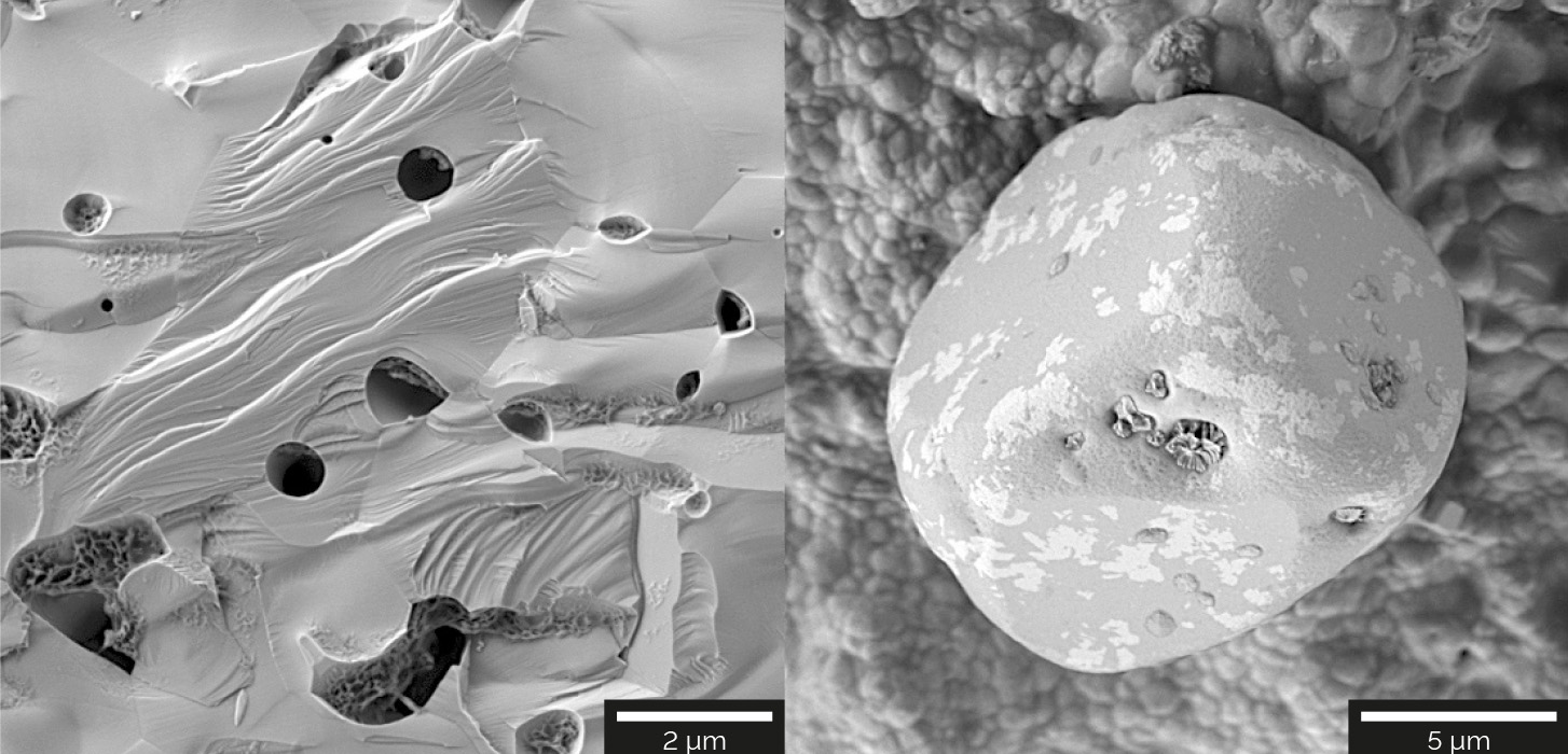
- Ceramic samples imaged with the E-T detector for topographic and material contrast. The ceramic sample on the left was imaged at 2 keV. The ceramic sample on the right was imaged at 500 eV for enhanced surface sensitivity.