
July 22, 2026
How Micro-CT Revealed New Insights into the 2,400-Year-Old Tollund Man
Discover how non-destructive micro-CT imaging revealed new insights into the 2,400-year-old Tollund Man and archaeological research.
Discover Tescan’s newest innovations, industry insights, and expert updates shaping the future of electron microscopy.
Discover how non-destructive micro-CT imaging revealed new insights into the 2,400-year-old Tollund Man and archaeological research.
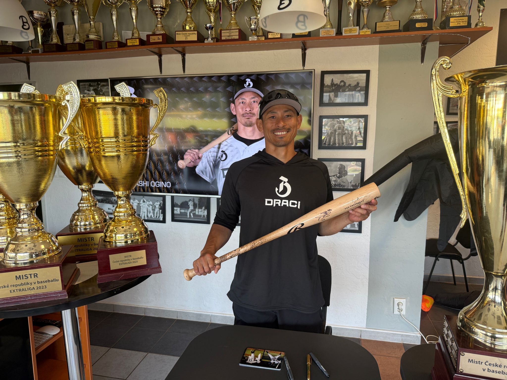
Discover how Micro-CT revealed the internal condition of a baseball bat after 2,000 swings using non-destructive 3D X-ray imaging.

Discover how Tescan grew from a small team in Brno into a global leader in electron microscopy and scientific instrumentation.

Discover how Tescan TIMA™ automated mineralogy helped researchers analyze Chang'e-6 lunar samples and refine our understanding of the Moon.

Learn how 4D micro-CT reveals freeze-drying dynamics and helps researchers study structural changes non-destructively.

Discover how integrated argon polishing improves TEM lamella preparation, repeatability, and FIB-SEM specimen quality.

An interview with Stanislav Haviar on 4D-STEM in SEM, thin-film materials research, and how Tescan AMBER 2 supports advanced characterization workflows.
.png?width=400&height=277&name=Tescan-news%20(3).png)
Tescan announces the winner of the UniTOM® XL Dynamic CT Beam Time Competition 2026 and the selected carbonate dissolution research project.

Learn how researchers at TUM use micro-CT to study food drying, plant-based foods, root-soil interactions, and dynamic processes.

Learn how micro-CT enables non-destructive 3D and 4D imaging, helping researchers visualize internal structures and dynamic processes.
-1.png?width=400&height=277&name=image%20(5)-1.png)
Learn why FIB-SEM is the preferred method for TEM specimen preparation, enabling site-specific targeting, faster workflows, and reliable results.

Discover how researchers at the University of Žilina use electron microscopy and Tescan MIRA XR to study metallic materials, fractography, structural changes, and industrial failures

Learn how a scanning electron microscope (SEM) works using the simple analogy of the Battleship game. Explore SEM signals, raster scanning, and FIB-SEM workflows.

Discover how Tescan’s integrated retractable 4D-STEM detector enables diffraction-based analysis directly in SEM and FIB-SEM workflows for advanced materials characterization.

Discover how Micro-CT, ultrafast laser processing, and FIB-SEM create a faster, more reliable failure analysis workflow for advanced semiconductor packaging.

Learn the fundamentals of sample preparation in electron microscopy, including cleaning, coating, mounting, TEM lamella preparation, and cryo-EM workflows.

Learn how TEM lamella thickness and window width influence stability during FIB preparation. Practical guidance for reducing bending, uneven polishing, and punch-through risk.

Discover how FemtoChisel™ laser solutions enable precise and efficient sample preparation workflows, supporting advanced microscopy and materials analysis.

Learn how integrating low-energy argon ion beam cleaning with Ga+ FIB-SEM improves (S)TEM sample preparation by reducing damage and enabling high-quality nanoscale analysis.

Learn the fundamentals of electron microscopy, including how SEM, TEM, and STEM work, how images are formed, and what signals reveal about materials at the nanoscale.

An interview on CEITEC Nano infrastructure, plasma FIB-SEM with SIMS, and advanced materials workflows using Tescan AMBER X 2.

Explore how Tescan TIMA™ enables automated mineral mapping and phase identification in geological samples from Kerguelen Island using advanced mineralogy workflows.

Learn how automated mineralogy and Tescan TIMA help mining teams make faster, decision-ready processing choices. Insights from mineralogist Braam Smit.

Discover how micro-CT supports embryology and fetal imaging in clinical environments. Insights from Bernadette de Bakker on 3D imaging, research, and care.
.png?width=400&height=277&name=News-feature-image%20(5).png)
Learn what STEM (Scanning Transmission Electron Microscopy) is, how it works, and how it compares to TEM. Explore 4D-STEM, electron diffraction, and analytical techniques for materials and semiconductors.

The INDICO FEBID workshop in Frankfurt advanced digital control for reliable 3D nanoprinting. Tescan contributed expertise in SEM-based nanofabrication, FIBID and in situ process monitoring.

Discover how micro-CT imaging is transforming prenatal care and early human development research through non-destructive, high-resolution 3D anatomical analysis.

Discover how 4D-STEM and TESCAN TENSOR enable dose-efficient analysis of beam-sensitive materials, advancing electron diffraction and structural research.
Submit your proposal for one week of dynamic X-ray CT beam time on Tescan UniTOM XL in Warrendale, PA. Deadline: 31 March 2026.

Discover how integrating micro-CT and plasma FIB-SEM enables multiscale 3D characterization of heterogeneous materials, linking structure, and performance.
.png?width=400&height=277&name=Untitled%20design%20(9).png)
Learn how to reduce EBL stitching errors on a standard SEM using technological layers and smart write-field placement in a GDSII workflow.

Learn practical methods to estimate lamella thickness for TEM, including FIB-SEM transparency, EELS-based measurement, and X-mark polishing techniques.

An interview with Riley Tejcek on performance and safety, including how non-destructive X-ray CT supports materials inspection in demanding environments.

Dr. Tatiana Gorelik shares insights on 3D electron diffraction, data acquisition strategies, and how new instrumentation shapes crystallography research.
Carlyle and Shimadzu Corporation have signed an agreement under which Tescan would become part of Shimadzu, subject to regulatory and customary approvals. The transaction has not yet closed.
.webp?width=400&height=277&name=MICRO_UniTOM_XL_2%20(2).webp)
The University of Defence in Brno installs Tescan UNITOM XL microCT for ballistic protection, composite materials research, and advanced 3D material analysis.
.png?width=400&height=277&name=Frame%20714%20(2).png)
Remove bottlenecks in TEM workflows by taking lift-out outside the FIB-SEM and into a dedicated EXLO station

Tescan and Wirsam co-hosted a hands-on Mineralogy Workshop in Johannesburg, uniting TIMA users to share insights on automated mineralogy and data optimization.

Discover the main topics of iCT 2026 in Linz and how Tescan will share new ways to improve micro-CT imaging, workflows, and research outcomes.

See the key trends from ISTFA 2025, including advances in semiconductor failure analysis, laser sample preparation, and workflow improvements for modern devices.

Czech Technical University enhances construction materials research with the Tescan AMBER X FIB-SEM, unlocking advanced microstructure analysis and 3D tomography capabilities.

Tescan UK will join the SEMT Meeting 2025 at the Natural History Museum in London, connecting with the microscopy community to discuss imaging workflows and innovations.

SGS celebrates the 100th TESCAN TIMA installation in Chile, advancing automated mineralogy and high-throughput mineral characterization.

Tescan showcased new technologies, AMBER X2, and TENSOR at the National CEMS Conference 2025, highlighting innovation in electron microscopy and workflow efficiency.

Tescan and Dragonfly Energy showcase how advanced microscopy and data analytics accelerate lithium-ion battery innovation and sustainable manufacturing.

Dr. Jana Jurmanová from Masaryk University discusses how the TESCAN CLARA electron microscope supports materials research and student training.

Tescan joins Mikrolux at the 32nd Annual Meeting of the Croatian Microscopy Society in Zagreb to connect with researchers and share innovations.
Tescan supports the new Plasma FIB-SEM laboratory at CTU Prague, advancing materials science research and innovation in civil engineering.

Discover how Tescan’s cryo-electron microscopy workflow helped uncover algae’s adaptive response to ZnO nanoparticles in collaboration with Mendel University.

Tescan will join the Cryo-Microscopy Group Meeting at the University of Nottingham to showcase its Cryo SOLARIS X² system and latest cryo-microscopy innovations for life sciences.

Discover how Tescan showcased its latest developments in TEM lamella preparation, 4D-STEM analysis, and energy materials research at the CMC Workshop 2025.

Discover how Tescan’s workflow integration and regional expansion are transforming semiconductor analysis and packaging. Watch the DIGITIMES interview with Hervé Macé and Sean Lee.

Highlights from the 3rd Tescan Collaboration Network Meeting at ER-C

TESCAN joins October events in Heidelberg and Bochum — showcasing solutions for life sciences imaging and materials research. Visit our booths & talks.

University of Leeds and RMS hosted a 4D-STEM & 3D-ED workshop, featuring TENSOR demos, keynotes from global experts, and interactive scientific sessions.

Tescan Group today announced the acquisition of FemtoInnovations and the creation of a dedicated Laser Technology Business Unit (LT BU).

Remove bottlenecks in TEM workflows by taking lift-out outside the FIB-SEM and into a dedicated EXLO station

At IPFA 2025, Tescan presented cutting-edge FIB-SEM & Micro-CT platforms solving semiconductor failure analysis, yield, and reliability challenges.

TESCAN’s AMBER X 2 Plasma FIB-SEM wins the 2025 R&D 100 Award for combining high-throughput 3D analysis with nanometer-precision TEM specimen prep.
.jpg?width=400&height=277&name=Microscopy-Conference(MC).jpg)
Tescan Group proudly introduces its new global brand platform The Art of Discovery at this year’s Microscopy Conference (MC) in Karlsruhe, Germany.

TESCAN will co-host a collaborative webinar with the University of Leeds, presenting a low-dose 4D-STEM methodology for characterising beam-sensitive polymers and soft matter.

Tescan introduces AutoSection and TEM AutoPrep PRO at M&M 2025 - accelerating semiconductor workflows through precision automation and user-friendly software.