
Insights
The importance of visualizing complex details in your sample and using them in their full context
In the current opinion-rich media environment, providing contextual background to the data that underlies opinions is equally, if not more, important than providing the opinion itself. The same is true for microscopy, which tempts scientists and engineers to focus only on the tiniest details in the materials they investigate. But, suppose the cross section prepared by FIB is too small and made at a location without defects? Or a 3D tomography is performed on a small volume at a shallow depth, revealing small grains overall? In both cases, the lack of context may lead to inaccurate conclusions.
Learn why visualizing complex details in your sample and using them in their full context is crucial for accurate conclusions in our latest paper!
2D/3D UHR FIB-SEM characterization of materials
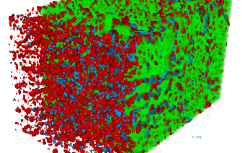
FIB-SEM is designed to perform site-specific cross-sectioning, sample fabrication and sample modification with an ion beam, either gallium FIB or Xe plasma FIB. This extends characterization to below the sample surface. The ability to use FIB to precisely remove material permits access to the sample’s Z dimension, leading to more comprehensive data from the sample.

Obtain the best 3D characterization data from any sample


Detect light elements at ppm concentrations such as Li or C in Battery Research


Maximize samples characterization throughput for your 3D volume analysis
TEM sample preparation for STEM/TEM analysis
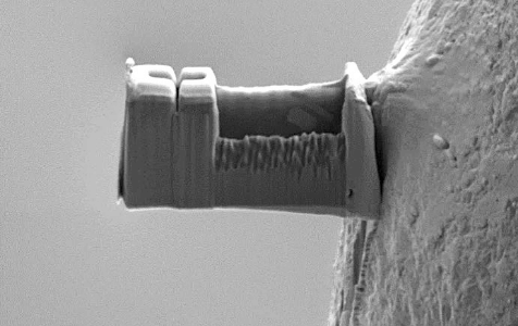
The success of transmission electron microscopy (TEM) analysis depends heavily on the quality of the sample preparation, especially when atomic resolution is needed or when material features are smaller and more complex. Using FIB to prepare samples for TEM provides the best method for achieving the required thin lamella and ensuring uniform quality.

Prepare TEM specimens consistently in high quality without being a FIB-SEM expert


Prepare highest quality TEM specimens even from highly demanding samples


Mitigate polishing artifacts such as scratches and curtaining
Nanoscale prototyping and nanofabrication
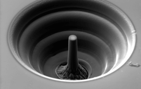
Many products in microelectronics, automotive or scientific equipment were previously prototyped and fabricated at the nanoscale. Nanoscale fabrication is often the subject of fundamental materials science and has resulted in many practical applications, such as sensors for self-driving cars, biomimetic materials and many enhancements in the microelectronics industry.

Prototype micro- and nano-devices like micropillars, cantilevers and microfluidic channels


Prepare nanofabricated structures from any Material

Create three-dimensional nanopatterns like plasmonic half helix resonators