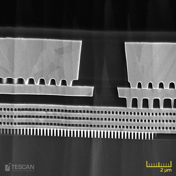
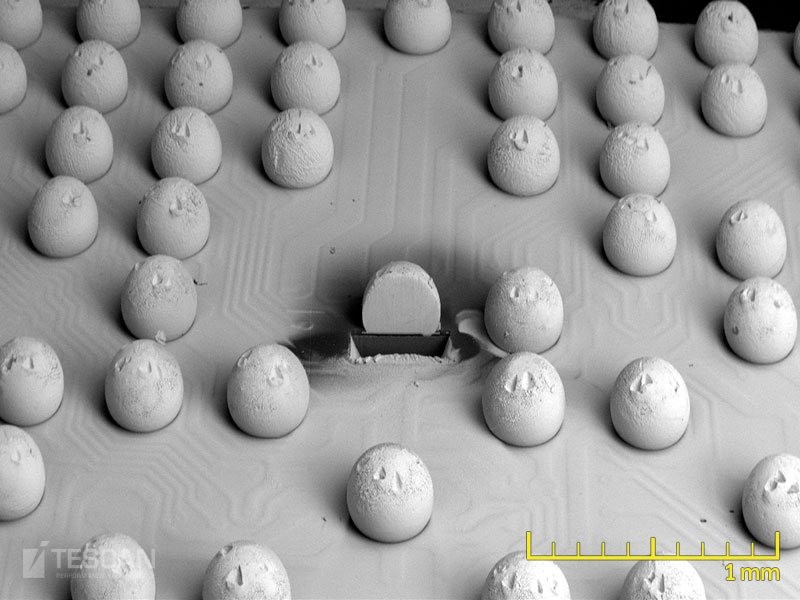
BGA makes high density and efficient use of the printed circuit board (PCB) possible. This is because the entire underside of the chip package can be used for connectivity as opposed to wire bonding or quad flat pack (QFP) where connections are only made around the periphery of the chip. Additionally, solder balls provide shorter connections which reduce signal inductance, resulting in less noise voltage and thus improved performance. For BGA to be properly soldered, a precise amount of heat needs to be applied so that each ball in the grid adequately melts and a good quality connection is made. The aim of BGA inspection is to detect and isolate defects that originated during the manufacturing process such as voids or badly soldered balls and their causes.
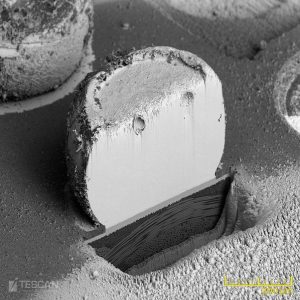
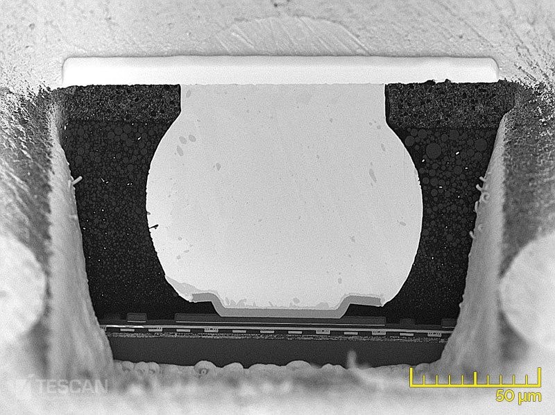
Cross-section of a solder ball with a diameter of 400 μm completed in 4 hours using Xe Plasma FIB and Rocking Stage for a curtaining-free surface
- TESCAN systems offer a wide range of possibilities for inspection and failure analysis of BGA packaging.
- The TESCAN EBIC detector can be used for electrical tests. More rigorous tests require the analysis of the solder balls themselves.
- The TESCAN BSE detector provides high contrast which makes intermetallic compounds and under-bump metallurgy layers clearly visible. The inspection and characterisation of solder ball junctions in BGA are crucial tasks to determine the reliability of an integrated circuit attached to a PCB and critical in determining the quality of the soldering process and when identifying the cause of the failure.
- TESCAN Plasma FIB-SEM systems allow solder balls, which can have diameters of up to hundreds of microns, to be effortlessly cross-sectioned in an unrivalled short time frame.
- Additionally, 3D microanalysis (3D EDX, 3D EBSD) of whole solder balls, for revealing voids, brittle fractures, die cracking or dendritic structures are possible with the ultra-high sputtering rates that only the Xe plasma FIB can offer.
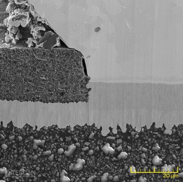
- A detailed image showing grain contrast in the pad metal and under-bump metallurgy layers
- A cross-section of a solder ball milled from the board side
- A cross-section of a solder ball milled from the board side
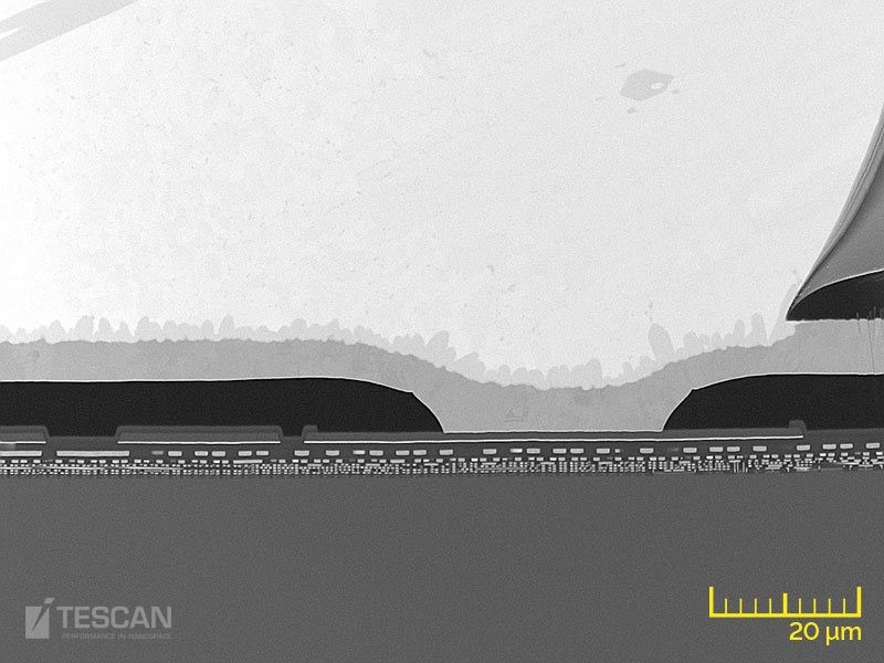
- BSE image of a cross-section of a solder ball showing intermetallic compounds between the solder and metal pad, polyimide passivation, and underlying IC layers
- Detailed image of a structure under the solder ball
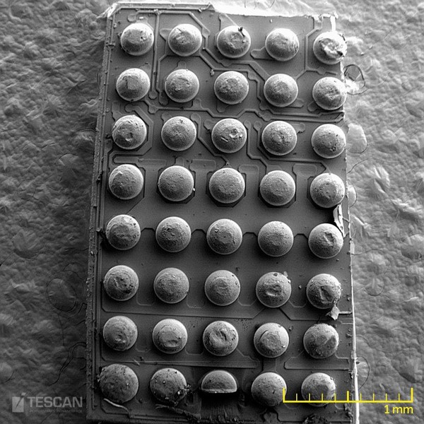
- Overview of a solder ball array
- Cross-section of a solder ball with a diameter of 400 μm completed in 4 hours using Xe Plasma FIB and Rocking Stage for a curtaining-free surface


