Displays can be of two types: thin-film transistor liquid crystal displays (TFT-LCD) or based on organic compounds light-emitting diodes (OLED) that offer high-quality image at low power consumption. LCD and OLED displays incorporate both extremely hard materials (molybdenum and titanium nitride) and extremely soft materials (silver alloys). An SEM analysis of these structures is complicated because of the thickness of glass (or plastic) substrates, organic interlayers, and integral touch screens.
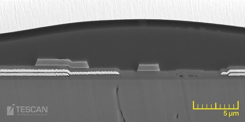
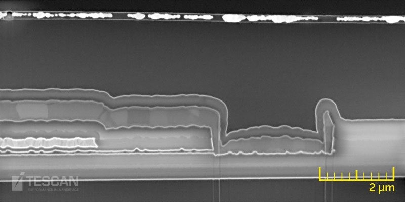
Cross-section of metal contacts and data lines in a TFT array prepared with a Ga source FIB
- TESCAN offers a series of instruments well-suited for the display industry. Displays are delicate structures which can be easily damaged by an electron beam.
-
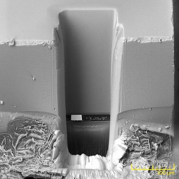
- TFT panel large-area (more than 300 µm depth) backside milling performed with plasma FIB
-
- BSE image showing microstructures of the various AMOLED conductive and insulating layers
-
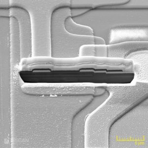
- Cu bumps and metallization between thick Si and glass layers in a TFT panel
-
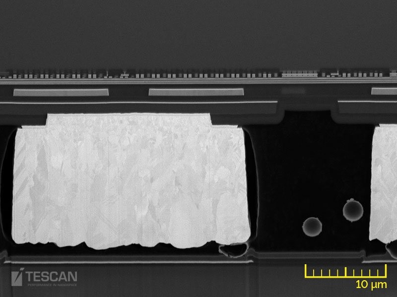
- OLED display layer inspection: an underfilled layer at the top