Such integrated circuits are multilayer structures whose key elements are multi-gate transistors, where a source-drain channel („fin“) is surrounded by a 3D gate.
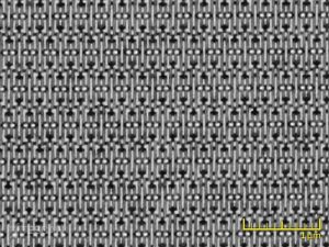
14 nm technology node Intel processor. A top view of the transistor contact layer after delayering by GIS-assisted Xe Plasma FIB etching, image obtained at an electron accelerating voltage of 500 V with the In-Beam detector
- A failure analysis process of such integrated circuits typically involves delayering and electrical nano probing. After the defective area is found a lamella containing the failure of interest can be prepared for TEM inspection.
- So far, delayering has been performed mainly by means of mechanical polishing. However, for future devices, mechanical polishing cannot be used due to micro and nanomechanical deformation and chemical interactions with polishing suspension.
- TEM lamella preparation is done on FIB-SEM systems. These lamellae must be artefact-free with the thickness proportional to the technology node.
Failure analysis of integrated circuits typically includes:
- Delayering and electrical probing in technology nodes of the last generation
- Preparation of TEM lamella from integrated circuits
- FIB-SEM tomography for 3D structural analysis (3D BSE reconstructions)
- Electrical fault isolation (EBIC, EBAC)
- Low voltage SEM inspection
-
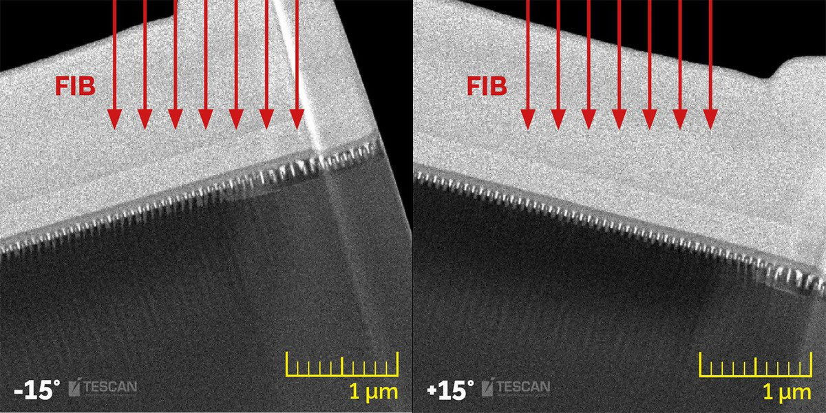
- 14 nm technology node Intel processor. Rocking Stage helps to mitigate curtaining on the TEM lamella by consecutive tilts of the sample to +/- 15° during lamella thinning
-
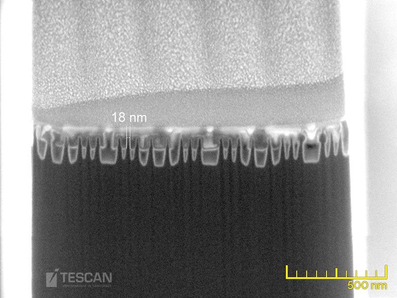
- A 14 nm technology node Intel processor. A side-view (“Fin-cut”) of a lamella during thinning, the final lamella was prepared just in the middle of a single fin (thickness less than 20 nm)
-
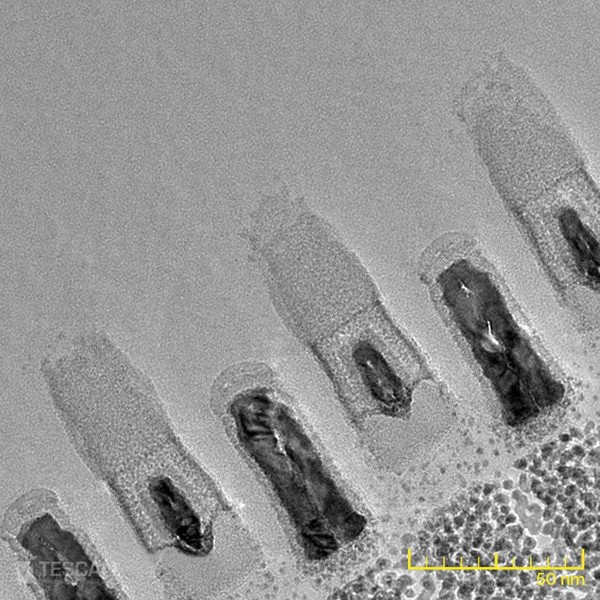
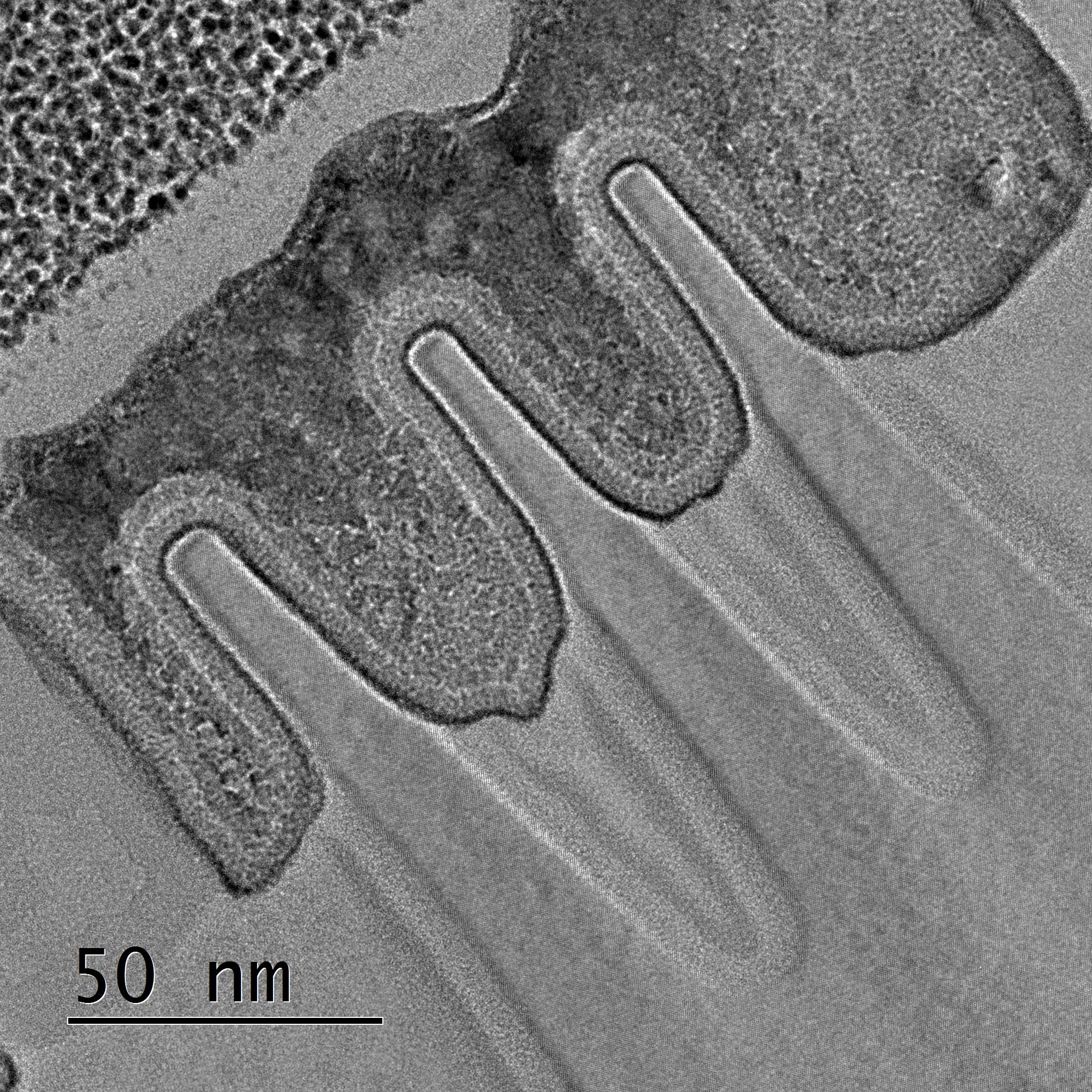
- High resolution TEM image of a gate-cut lamella prepared from a 14 nm chip by means of inverted thinning
-
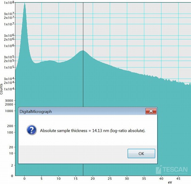
- A 14 nm technology node Intel processor. An EELS spectrum has confirmed the thickness of the lamella is below 15 nm
-
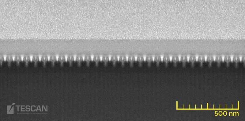
- A 14 nm technology node Intel processor. A cross-section showing the transistor layers (“Gate-cut”) imaged at 5 keV with the In-Beam detector.
-
- TEM image of a fin-cut lamella prepared from a 14 nm chip by means top-down thinning
-
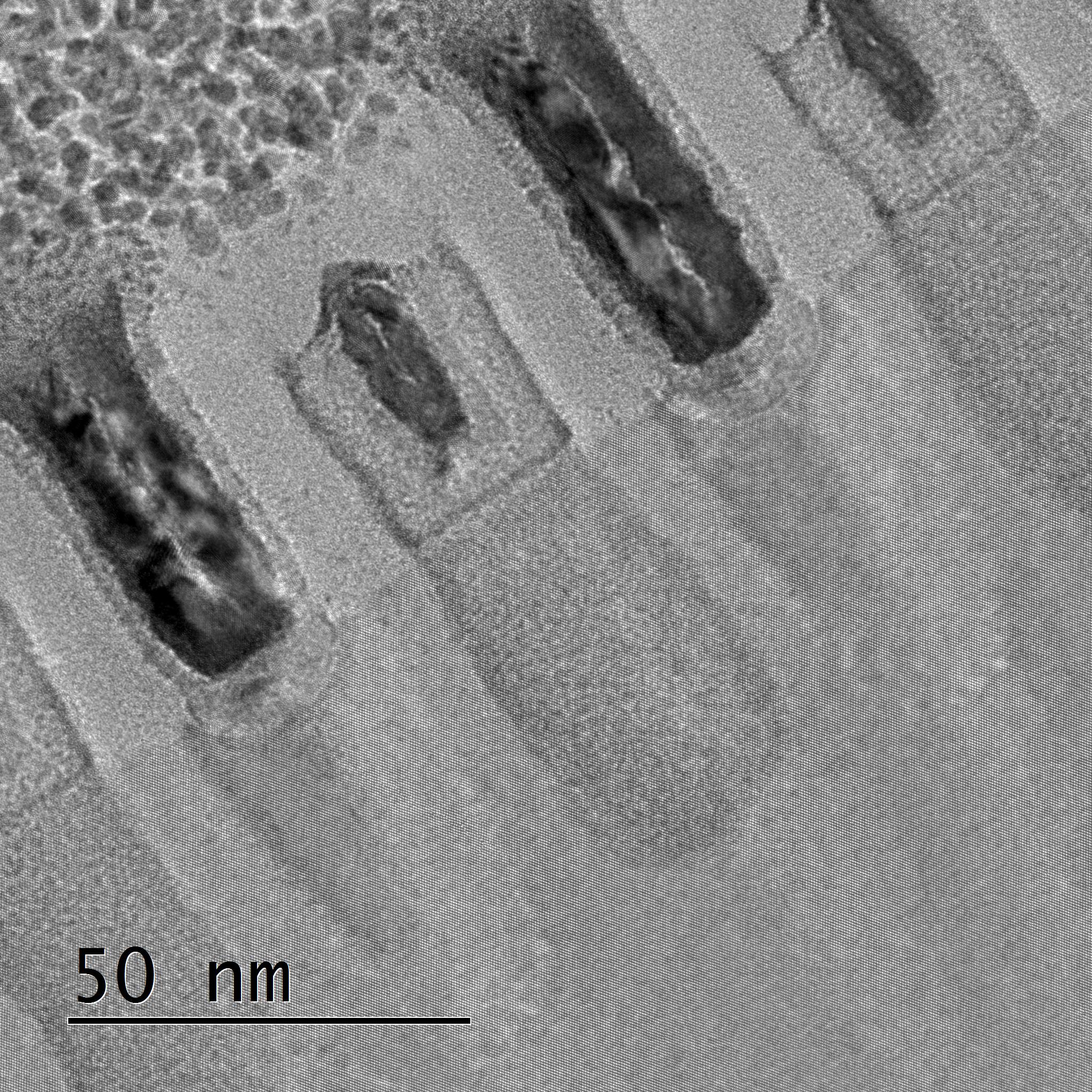
- TEM image of a gate-cut lamella prepared from a 14 nm chip by means top-down thinning on a Rocking stage
-
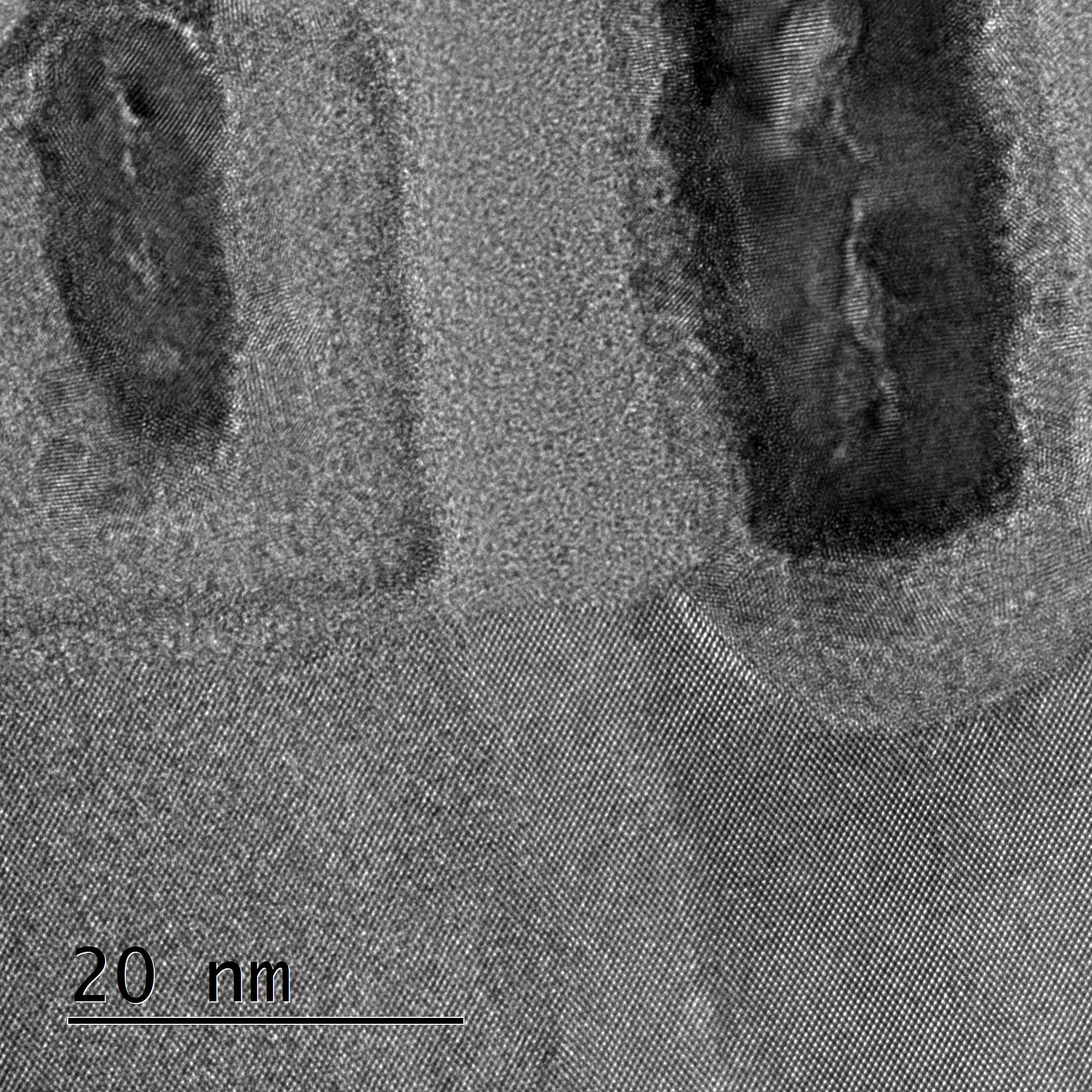
- High resolution TEM image of a gate-cut lamella prepared from a 14 nm chip by means top-down thinning on a Rocking stage