Diese integrierten Schaltungen bestehen aus mehrschichtigen Multi-Gate-Transistoren, bei denen ein Source-Drain-Kanal („Fin“) von einem 3D-Gate umgeben ist.
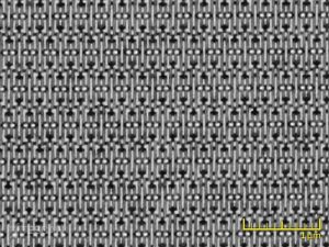
14 nm Technologie eines Intel Prozessors. Ansicht auf die Transistor-Kontaktschicht nach Freilegung durch GIS-unterstütztes Xenon Plasma FIB Ätzen, Bild aufgenommen mit 500 V Beschleunigungsspannung mit In-BeamSE Detektor
- Ein Fehleranalyseprozess solcher integrierter Schaltungen beinhaltet typischerweise das Freilegen und elektrisches Nanoprobing. Nachdem der defekte Bereich lokalisiert wurde, wird eine Lamelle, welche den Defekt enthält, für die TEM-Inspektion präpariert.
- Eine Freilegung wurde meist mittels mechanischer Politur durchgeführt. Bei modernen Bauelementen darf eine solche Politur wegen mikro- und nanomechanischer Deformationen und chemischer Interaktionen mit dem Politurmittel jedoch nicht mehr zum Einsatz kommen.
- Die TEM-Lamellenpräparation wird auf einem FIB-REM-System ausgeführt. Die Lamelle muss Artefakt-frei und in einer Dicke, proportional zur Technologiegröße, sein.
Fehleranalyse integrierter Schaltungen beinhaltet normalerweise:
- Delayering und elektrisches Messung in der Technologiegröße der neusten Generation
- Präparation einer TEM-Lamelle aus der integrierten Schaltung
- FIB-REM-Tomographie für 3D-Strukturanalyse (3D-BSE-Rekonstruktion)
- Elektrische Fehleranalyse (EBIC, EBAC)
- Inspektion mit dem REM bei niedriger Beschleunigungsspannung
-
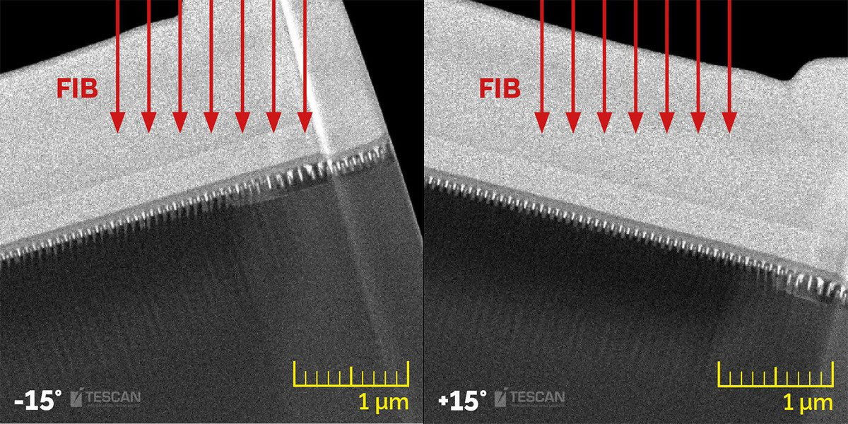
- 14 nm technology node Intel processor. Rocking Stage helps to mitigate curtaining on the TEM lamella by consecutive tilts of the sample to +/- 15° during lamella thinning
-
- A 14 nm technology node Intel processor. A side-view (“Fin-cut”) of a lamella during thinning, the final lamella was prepared just in the middle of a single fin (thickness less than 20 nm)
-
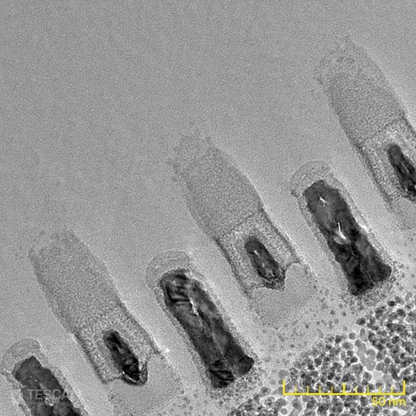
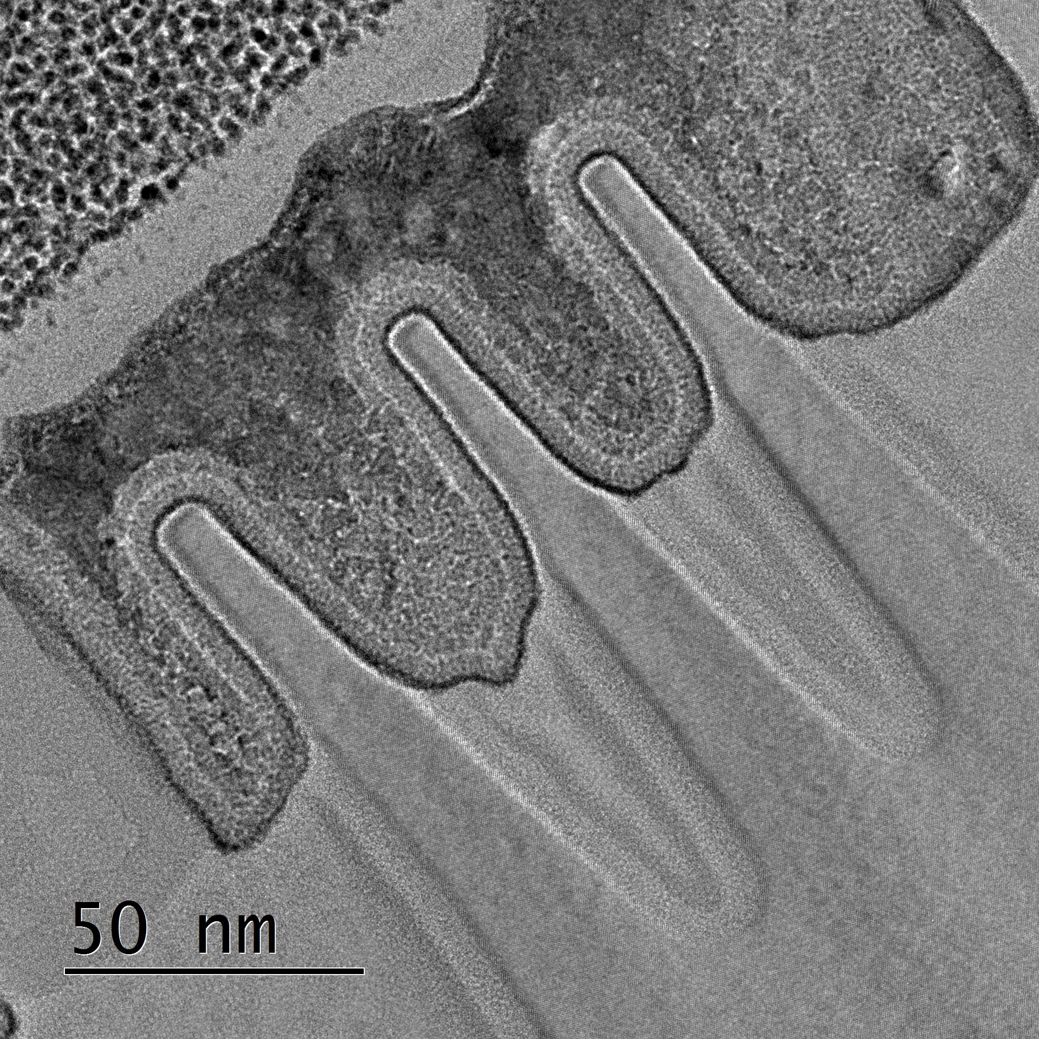
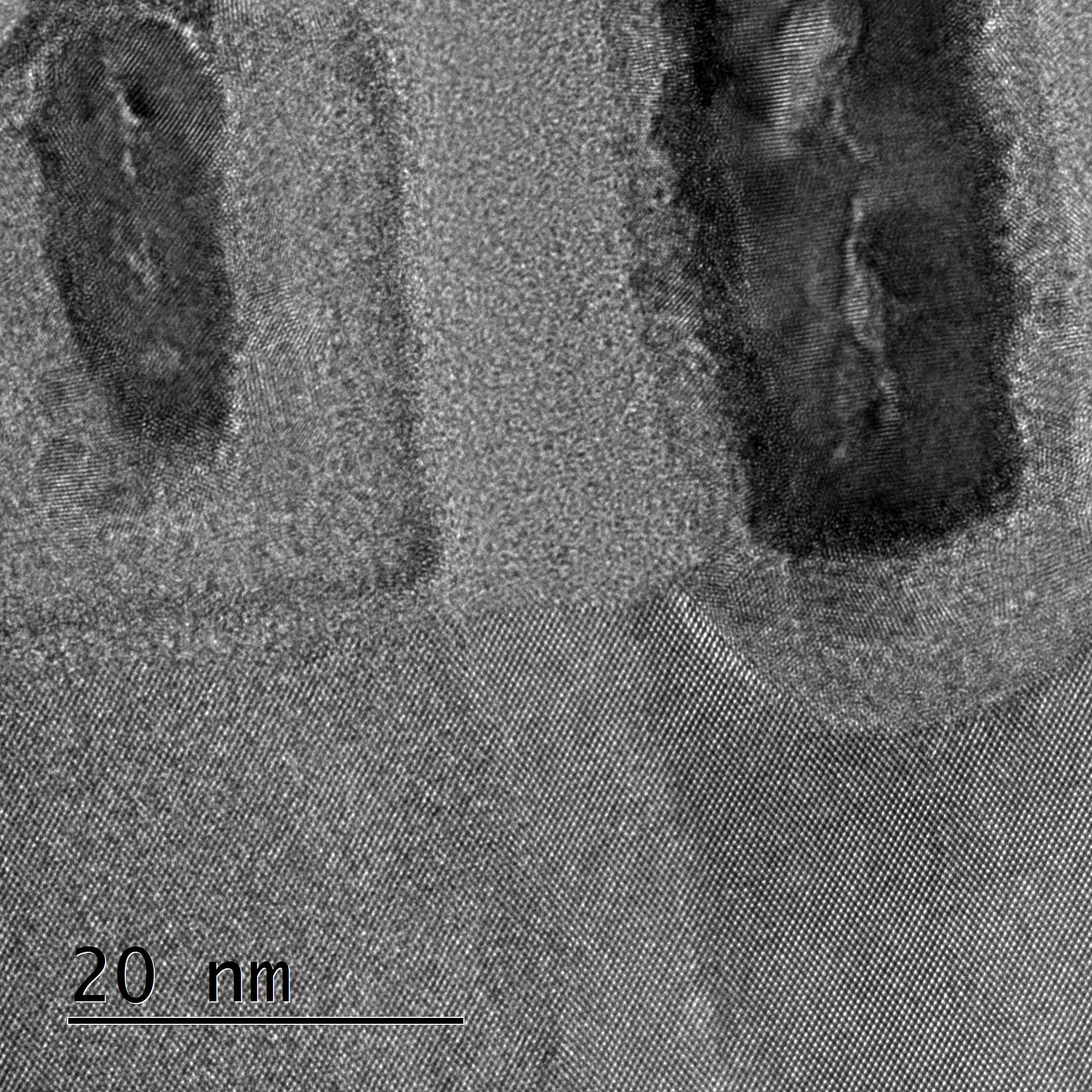
- High resolution TEM image of a gate-cut lamella prepared from a 14 nm chip by means of inverted thinning
-
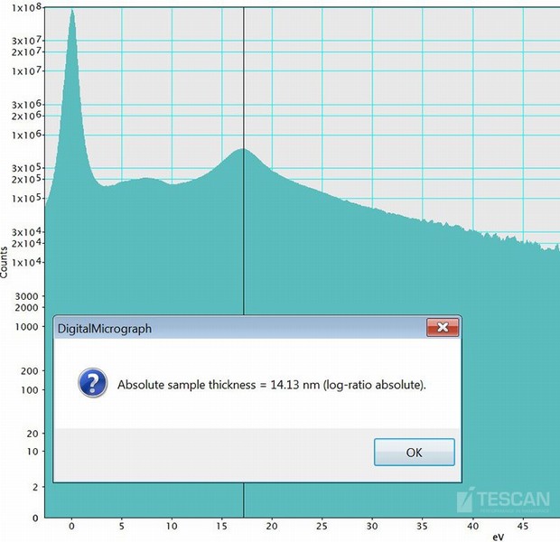
- A 14 nm technology node Intel processor. An EELS spectrum has confirmed the thickness of the lamella is below 15 nm
-
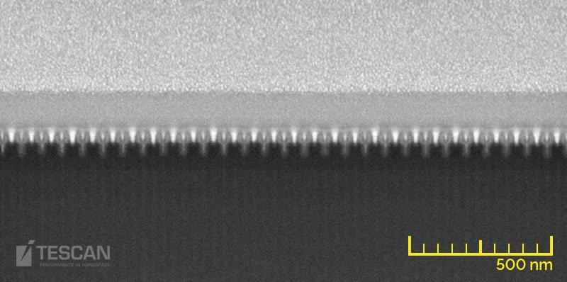
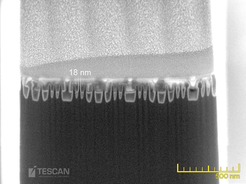
- A 14 nm technology node Intel processor. A cross-section showing the transistor layers (“Gate-cut”) imaged at 5 keV with the In-Beam detector.
-
- TEM image of a fin-cut lamella prepared from a 14 nm chip by means top-down thinning
-
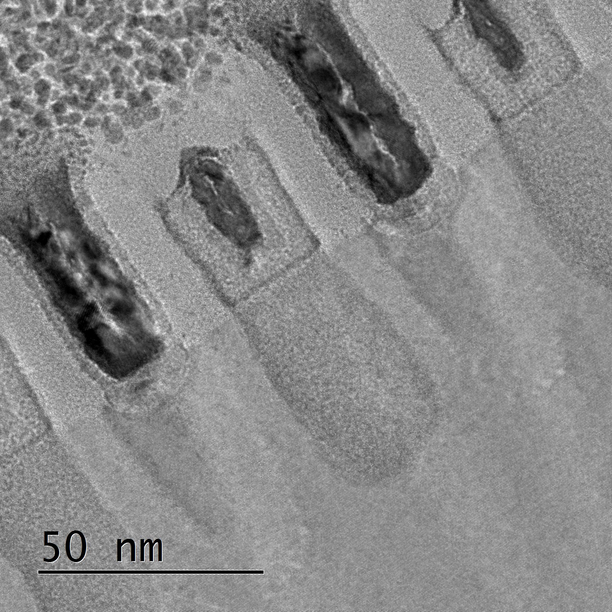
- TEM image of a gate-cut lamella prepared from a 14 nm chip by means top-down thinning on a Rocking stage
-
- High resolution TEM image of a gate-cut lamella prepared from a 14 nm chip by means top-down thinning on a Rocking stage