Tescan FIB-SEM (Focused Ion Beam Scanning Electron Microscope) systems combine high-resolution electron imaging with precise ion beam modification to support advanced nanoscale characterization, sample preparation, and 3D analysis workflows. Designed for materials science, semiconductors, battery research, life sciences, and geoscience applications, Tescan FIB-SEM platforms help researchers move seamlessly from imaging to nanomachining, cross-sectioning, tomography, and analytical investigation within a single environment.
Users working with large or complex samples often face a trade-off between milling speed and analytical precision. Tescan FIB-SEM technologies build on long-standing expertise in focused ion beam development, including the introduction of the world’s first fully integrated Xe plasma FIB-SEM platform (Orsay Physic is part of Tescan now). This foundation continues to shape today’s workflows, enabling high-throughput large-volume processing alongside high-resolution imaging and precise nanoscale modification within a single system.
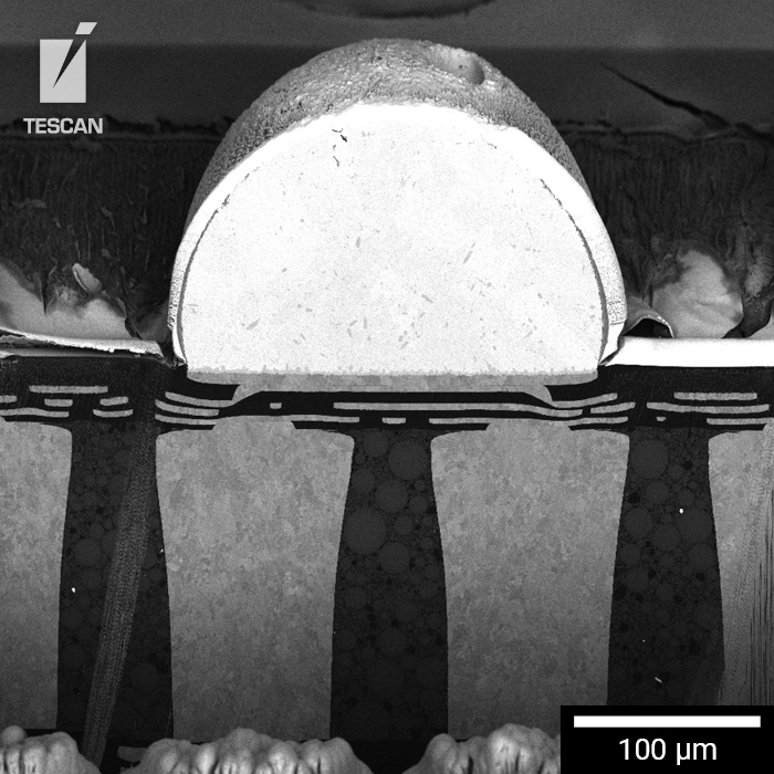
The portfolio includes both Ga⁺ focused ion beam systems for ultra-precise nanofabrication and TEM sample preparation, and Xe plasma FIB-SEM systems optimized for rapid large-volume milling and high-throughput workflows. Advanced plasma FIB technologies enable users to bridge the traditional gap between resolution and speed, supporting applications ranging from failure analysis and semiconductor process development to large-scale 3D characterization and multimodal materials analysis.
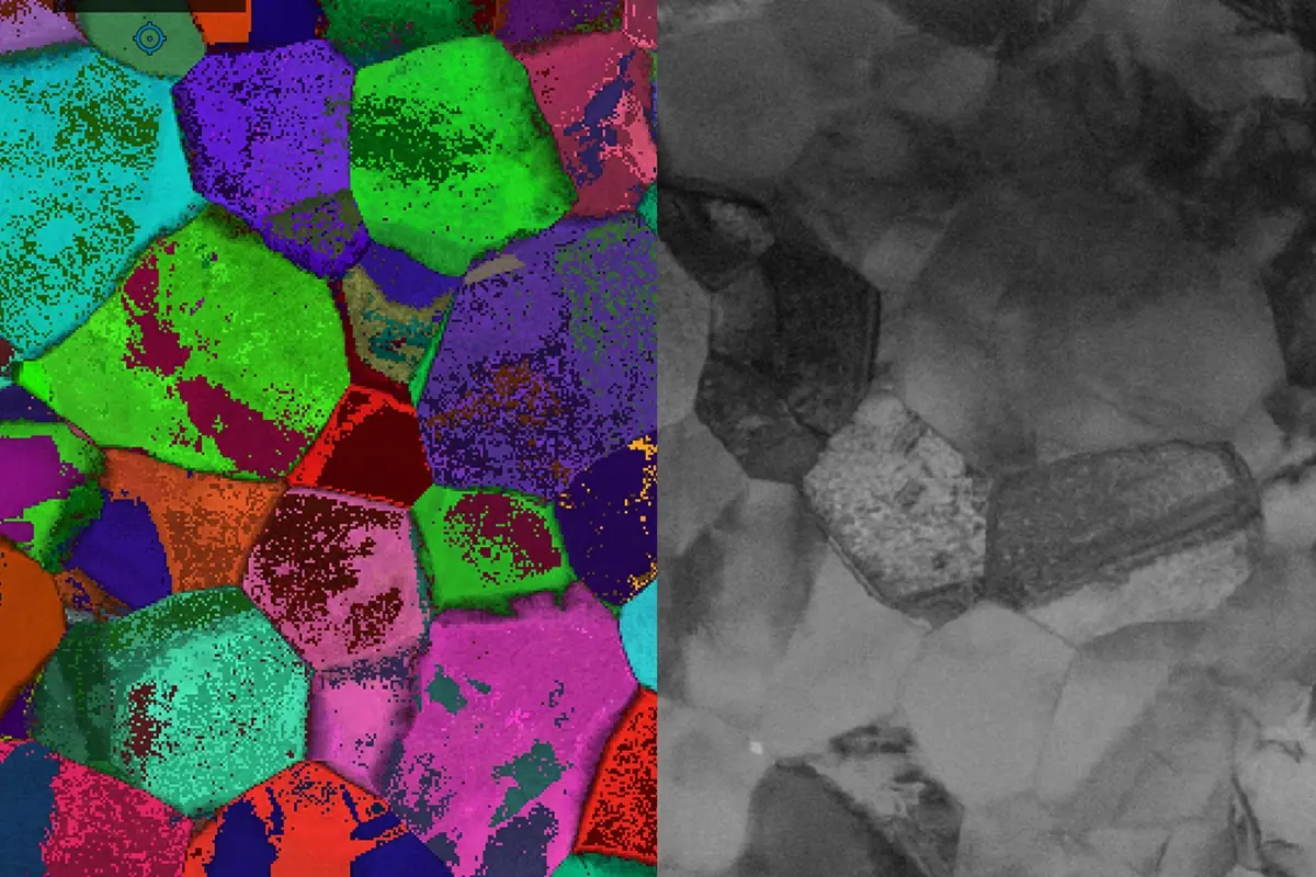
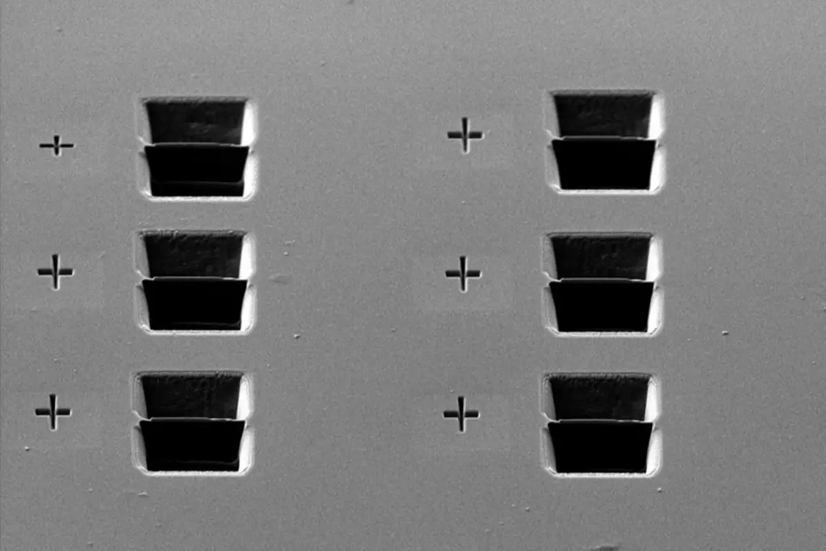
Tescan FIB-SEM solutions are engineered around modular architectures, field-free ultra-high-resolution SEM imaging, and flexible analytical integration including EDS, EBSD, ToF-SIMS, Raman, and in situ experimentation. Automated workflows for TEM lamella preparation, serial section tomography, and multidimensional correlative analysis help laboratories increase throughput while maintaining precision and reproducibility.
Not sure which FIB-SEM configuration best fits your application, workflow, or throughput requirements? Request a personalized consultation with a Tescan specialist to discuss your samples, analytical goals, and laboratory needs, and identify the solution best suited to your research or production environment.