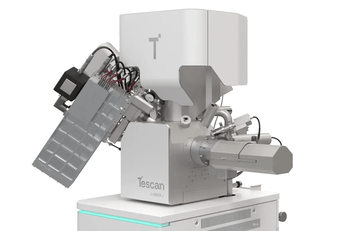
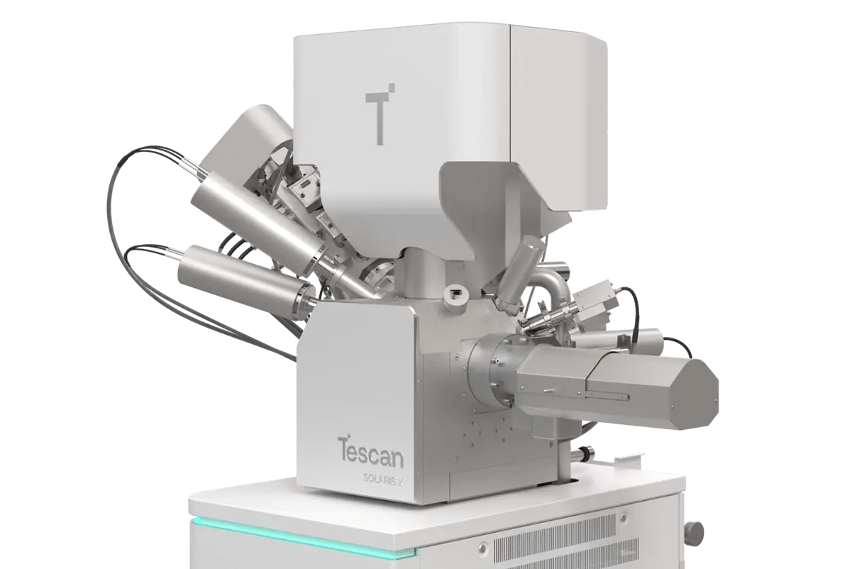
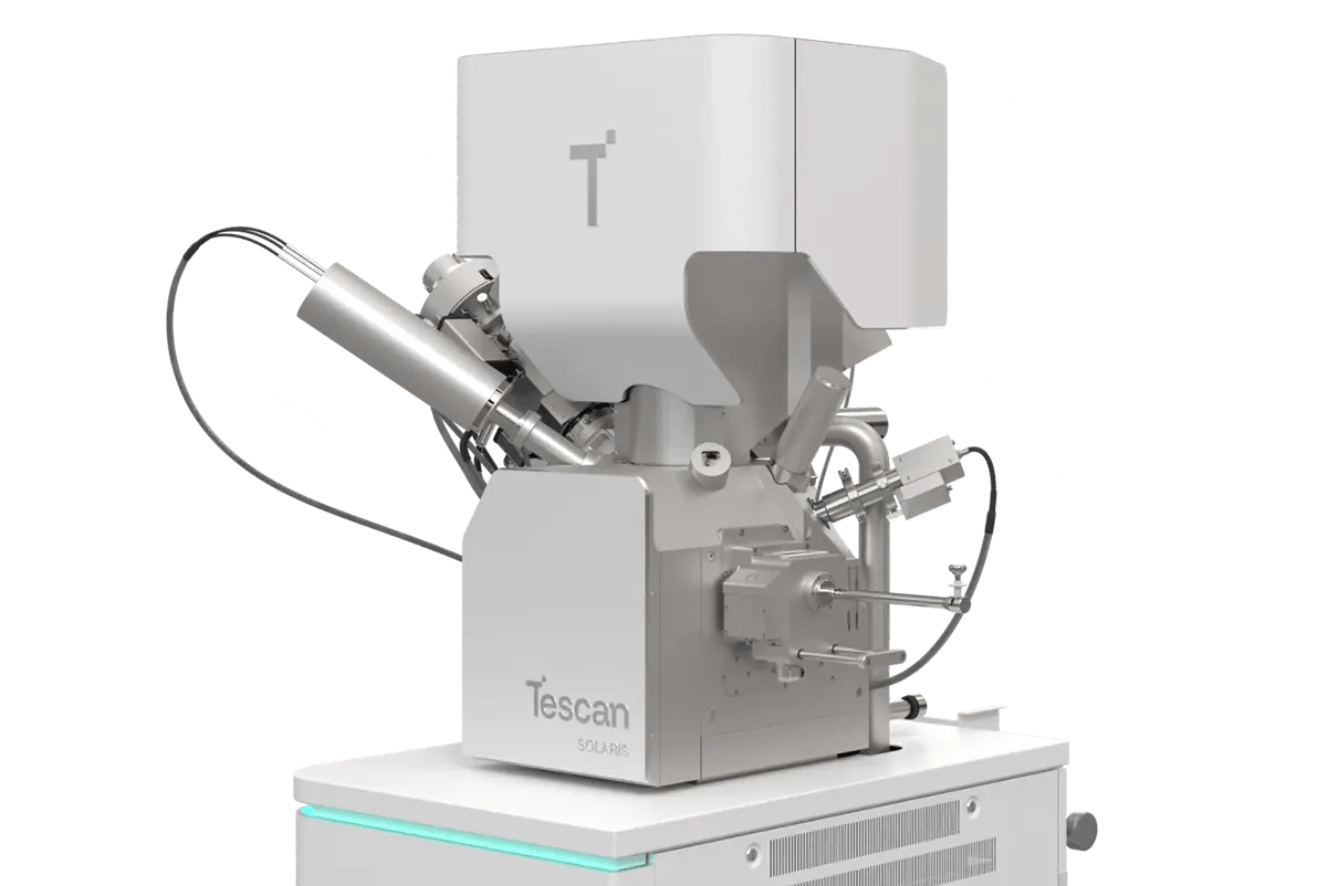
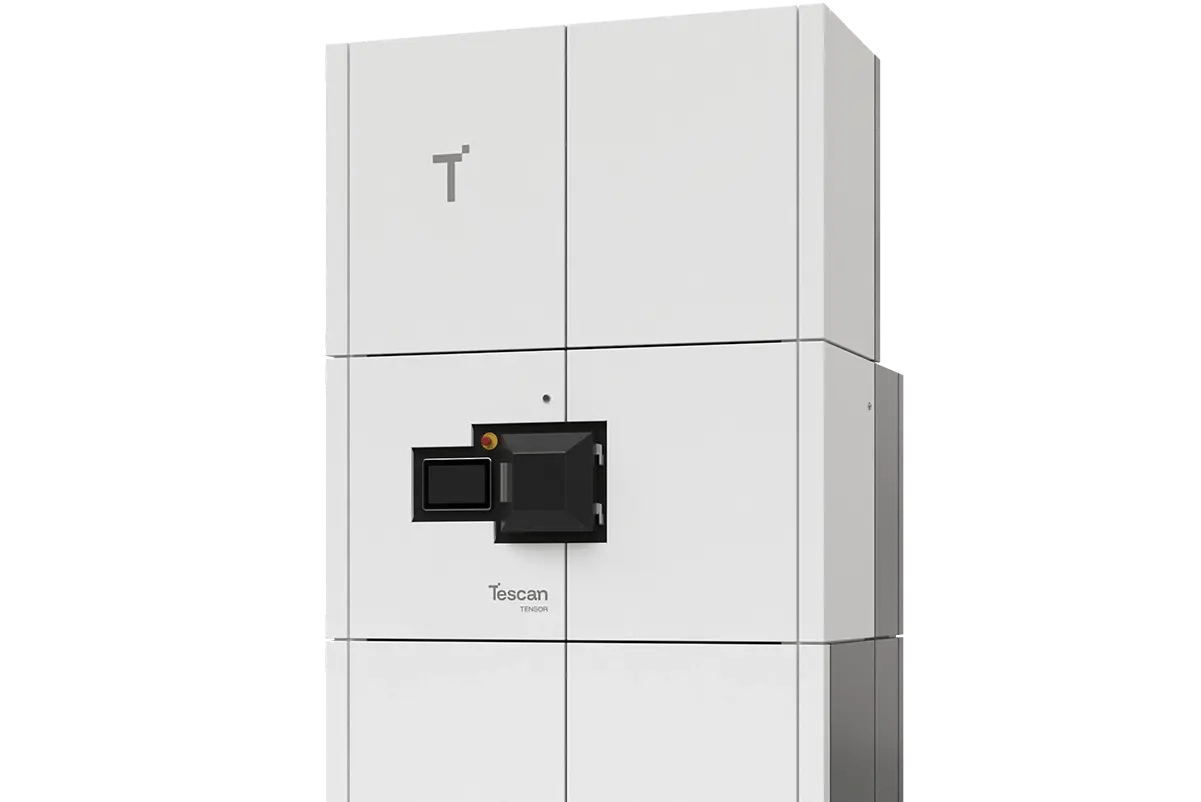
Achieve precise fault isolation in semiconductor failure analysis without damaging fragile device layers. Tescan FIB-SEM workflows deliver smooth delayering with plasma milling and CAD-assisted navigation.
Endpoint detection ensures you reach the circuit of interest without artifacts, while in situ imaging and probing streamline fault localization.
Enable reliable results that strengthen device performance and accelerate decision-making in semiconductor development.


_1x.webp?width=214&height=206&name=MicrosoftTeams-image%20(64)_1x.webp)


