X-ray ptychography – a high-resolution coherent diffractive imaging technique – was used to create three-dimensional images of complex multilayered integrated circuits with unmatched lateral resolution. The TESCAN FE-SEM Xe plasma FIB FERA3 system was used during the preparation process of the analysed samples.
-
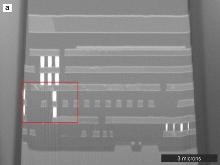
- Slice of the detector ASIC.