Visual inspection is an integral part of the production line in all semiconductor foundries. Most of the inspection techniques currently in use are optical-based which will face a resolution limit due to the continual reduction in the size of dies. TESCAN’s Image Snapper is a perfect substitution allowing non-destructive imaging based on the stitching of high-magnification images resulting in one high-resolution panorama image.
Download the new TESCAN Application Example and find out more on this.
-
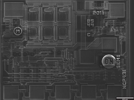
- The final high resolution panorama image consisting of 527 single images provides a very detailed overview of the entire die